An improved structure suitable for superjunction dmos devices

An improved structure and device technology, applied in semiconductor devices, electrical components, circuits, etc., can solve problems such as body diode reverse recovery is too hard, IRM and Qrr increase, prone to failure, etc., to increase the softness factor and slow down the current Decrease slope, improve the effect of reverse recovery curve

Active Publication Date: 2022-05-24
四川民承电子有限公司
View PDF15 Cites 0 Cited by
  • Summary
  • Abstract
  • Description
  • Claims
  • Application Information

AI Technical Summary

Problems solved by technology

[0004] Vertical super-junction power DMOS has good applications in many fields due to its low on-resistance, but in high-frequency applications, super-junction power DMOS shows some shortcomings
The study found that the columnar structure of the drift region brings two consequences to the body diode of super junction power DMOS: one is that the area of ​​the junction is much larger, which leads to the increase of IRM and Qrr when the body diode is injected forward; the other is that the first conduction type and the second conductivity type junction column to bring the body diode reverse recovery is too hard, prone to failure

Method used


Image

  • An improved structure suitable for superjunction dmos devices
  • An improved structure suitable for superjunction dmos devices
  • An improved structure suitable for superjunction dmos devices

Examples


Embodiment 1

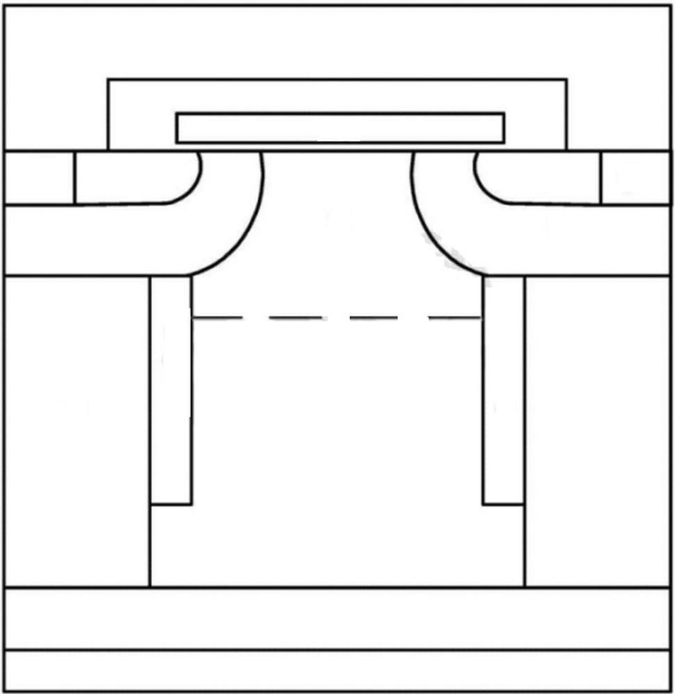
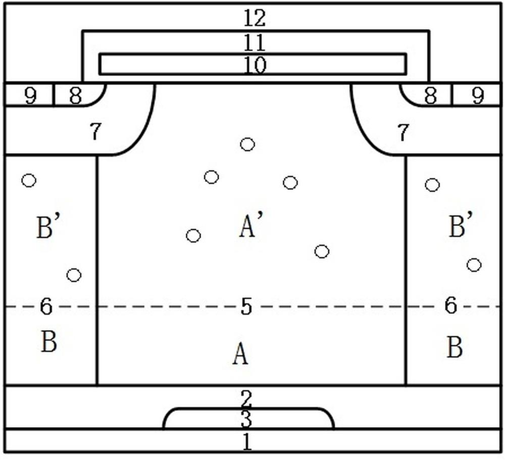
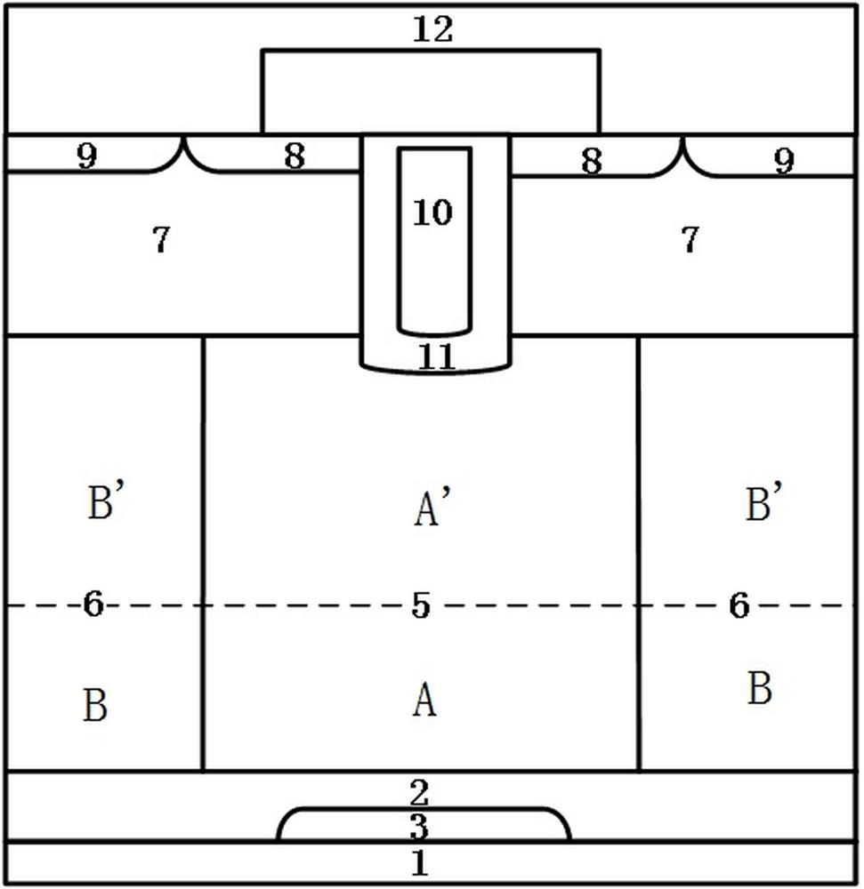
[0021] As a most basic embodiment of the present invention, such as figure 2 , this embodiment discloses an improved structure suitable for superjunction DMOS devices. A heavily doped semiconductor is also provided on the contact surface between the first conductive type semiconductor doped substrate 2 of the superjunction DMOS device and the metallized drain. The second conductivity type semiconductor island region 3, the heavily doped second conductivity type semiconductor island region 3 constitutes a hole injection region at the bottom of the device, and the heavily doped second conductivity type semiconductor island region 3 is embedded in the first The conductive type semiconductor doped substrate 2 and its bottom are also in contact with the upper surface of the metallized drain; and the first conductive type doped pillar region 5 and the second conductive type semiconductor doped pillar region 6 The carrier lifetimes are all longer than those in the upper half region....

Embodiment 2

[0024] As a preferred embodiment of the present invention, such as figure 2 , this embodiment discloses an improved structure suitable for superjunction DMOS devices. A heavily doped semiconductor is also provided on the contact surface between the first conductive type semiconductor doped substrate 2 of the superjunction DMOS device and the metallized drain. The second conductivity type semiconductor island region 3, the heavily doped second conductivity type semiconductor island region 3 constitutes a hole injection region at the bottom of the device, and the heavily doped second conductivity type semiconductor island region 3 is embedded in the first The conductive type semiconductor doped substrate 2 and its bottom are also in contact with the upper surface of the metallized drain; and the first conductive type doped pillar region 5 and the second conductive type semiconductor doped pillar region 6 The carrier lifetimes are all longer than those in the upper half region. ...


PUM


Abstract

The invention discloses an improved structure suitable for super-junction DMOS devices, which belongs to the technical field of electronic device optimization. A contact surface between the first conductive type semiconductor doped substrate and the metallized drain of the super-junction DMOS device is also provided. A heavily doped semiconductor island region of the second conductivity type, the heavily doped semiconductor island region of the second conductivity type constitutes a hole injection region at the bottom of the device, and the heavily doped semiconductor island region of the second conductivity type is embedded in the second A conductive type semiconductor is doped into the substrate and its bottom is also in contact with the upper surface of the metallized drain; The carrier lifetimes are longer than those in the upper half region.

Description

technical field [0001] The invention belongs to the technical field of electronic device optimization, and in particular relates to an improved structure suitable for a super-junction DMOS device. Background technique [0002] Power DMOS plays an important role in power conversion, especially in high-frequency power conversion, because of its fast switching speed, low loss, high input impedance, low driving power, and good frequency characteristics. The ever-increasing system performance requires power DMOSs with lower power losses and higher reliability under high electrical stress. DMOS device with super-junction structure is an important power device that has appeared in recent years. Its basic principle is the principle of charge balance. By introducing P-pillars and n-columns spaced from each other in the drift region of ordinary power DMOS. The super-junction structure of the column greatly improves the trade-off relationship between the on-resistance and the breakdow...

Claims


Application Information

Patent Timeline
Patent Type & Authority Patents(China)
IPC IPC(8): H01L29/78H01L29/06
Inventor 蔡少峰任敏高巍宋炳炎李科陈凤甫邓波
Owner 四川民承电子有限公司
Why Eureka
Try Eureka