
Patsnap Eureka
For R&D, Patsnap Eureka makes reading and utilizing patents & technical documents easy.
Patsnap Eureka AIR
Designed for self-driven R&D workflows. Generate viable solutions, solve complex R&D challenges, empower your innovation with AI.

Patsnap Eureka Materials
Designed for material experts only. Revolutionize your material R&D, from search, analyze, to developing new materials.

TechResearch
Generate reliable direction feasibility study reports for your R&D in just a few steps.

TechSeek
Discover and master advanced knowledge NOW. Basics, ideas, possibilities, all at once.

TechMind
As an expert in R&D Theories, TechMind can generates customized viable solutions instantly.

TechRisk
Analyze your overall solution with one click, know your potential R&D risks in advance.

TechMonitor
Get weekly tech updates, stay abreast of the latest tech innovations and key insights.
Circuit board and manufacturing method thereof
A manufacturing method and circuit board technology, which is applied in printed circuit manufacturing, printed circuit, printed circuit, etc., can solve the problems of unfavorable high-density circuit production and reduce the utilization rate of flexible circuit board typesetting, so as to increase the typesetting utilization rate and meet The effect of production requirements
- Summary
- Abstract
- Description
- Claims
- Application Information
AI Technical Summary
Problems solved by technology
Method used
Image

Examples
Embodiment Construction
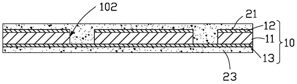
[0050] The following will be combined with Figure 1 to Figure 14 and an embodiment, the circuit board 100 provided by the technical solution and the manufacturing method thereof are further described in detail.
[0051] see Figure 1 to Figure 7 , the first embodiment of the present invention provides a method for manufacturing a circuit board 100, including the following steps:
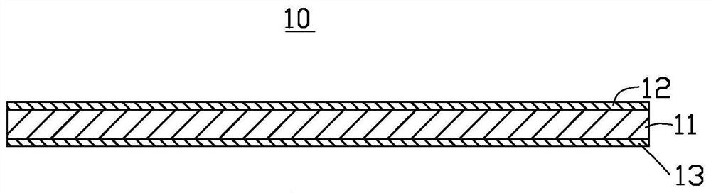
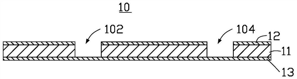
[0052] For a first step, see figure 1 , providing a substrate 10 .
[0053] The substrate 10 is double-sided, and the substrate 10 includes a base layer 11 , a first bottom copper layer 12 and a second bottom copper layer 13 formed on opposite sides of the base layer 11 .
[0054] In this embodiment, the base layer 11 is a flexible resin layer, such as polyimide (PI), polyethylene terephthalate (PET) or polyethylene naphthalate (PEN).
[0055] In the second step, see figure 2 , opening at least one connection hole 102 on the substrate 10 .
[0056] In this embodiment, the number of the connec...
PUM
 Abstract
Description
Claims
Application Information
 - R&D Engineer
- R&D Manager
- IP Professional
- Industry Leading Data Capabilities
- Powerful AI technology
- Patent DNA Extraction
Browse by: Latest US Patents, China's latest patents, Technical Efficacy Thesaurus, Application Domain, Technology Topic, Popular Technical Reports.
© 2024 PatSnap. All rights reserved.Legal|Privacy policy|Modern Slavery Act Transparency Statement|Sitemap|About US| Contact US: help@patsnap.com