Enhanced wave absorbing material structure body
A technology of wave-absorbing materials and structures, applied in the field of wave-absorbing materials, can solve the problems of poor heat dissipation performance of wave-absorbing materials and inability to take into account wave-absorbing performance, etc., achieve good heat dissipation effect, solve insufficient reflectivity, and good high power resistance sexual effect
- Summary
- Abstract
- Description
- Claims
- Application Information
AI Technical Summary
Problems solved by technology
Method used
Image
Examples
Embodiment 1
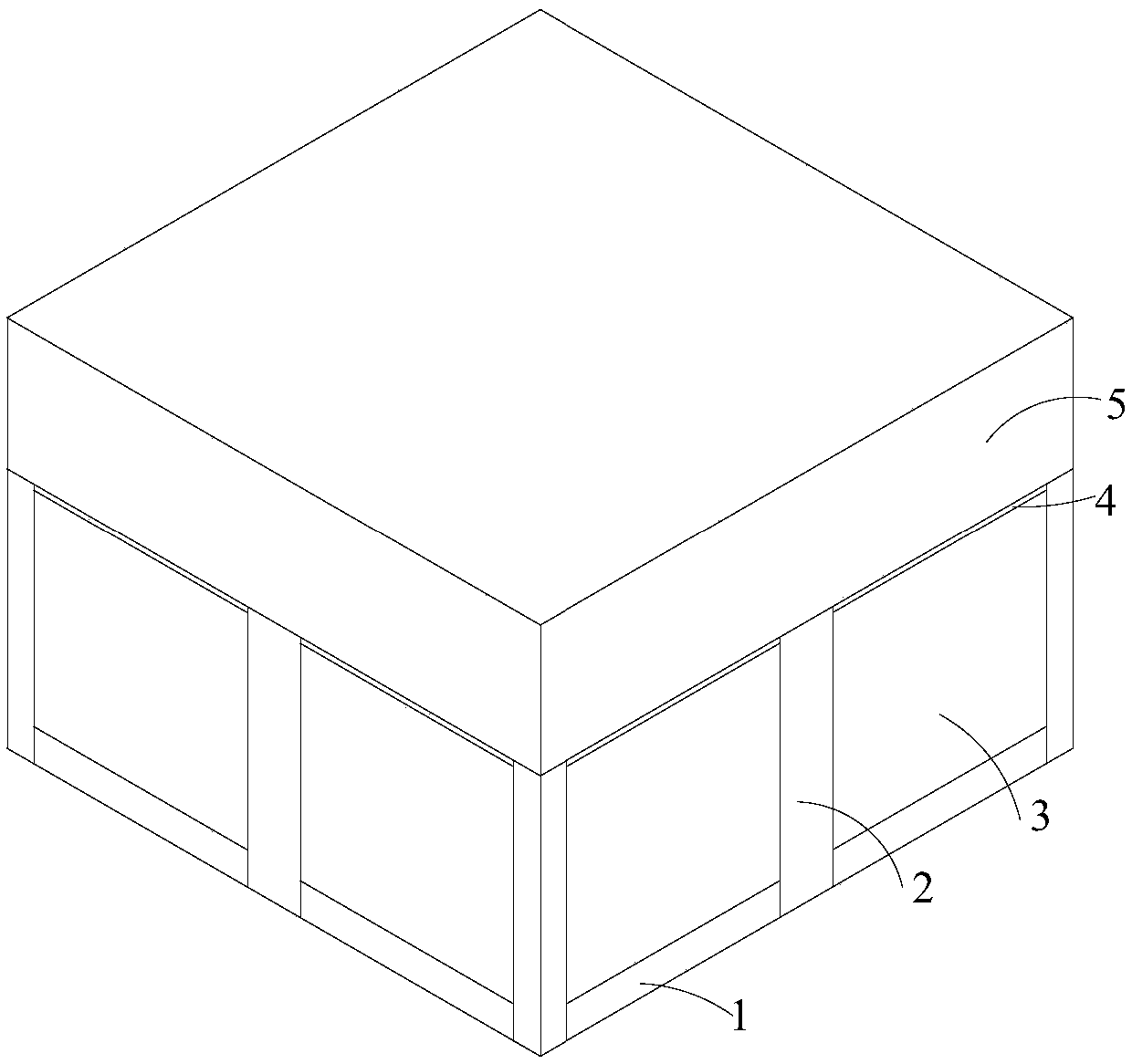
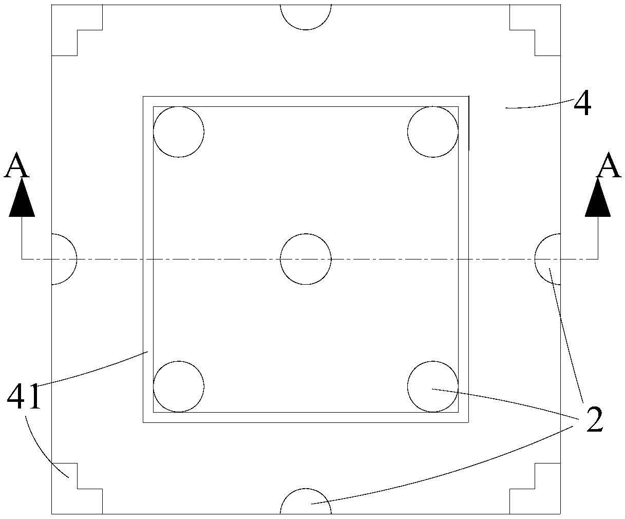
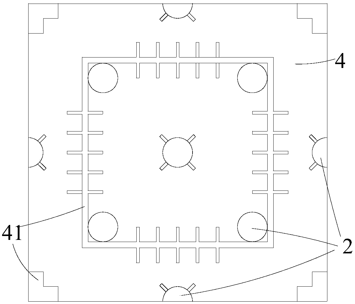
[0061] An enhanced wave-absorbing material structure, the enhanced wave-absorbing material structure is such as figure 1 , 2 , 4, the heat dissipation bottom plate 1 is a copper bottom plate with a thickness of 2mm; the heat transfer body 2 is a copper cylinder (no need to coat a thin layer of copper), and its radius is 1mm; the first wave-absorbing material 3 is an EPP material, Its length and width are 320mm×320mm, and its thickness is 22mm; the carrier board 4 is a PCB substrate board, its thickness is 0.3mm, its thermal conductivity is 0.4w / (m·℃), and its dielectric constant is 4.4; the reflection enhancement layer 41 is copper The foil layer has a line width of 0.5 mm; the second absorbing material 5 is an EPP material with a length and width of 320 mm×320 mm and a thickness of 8 mm.
Embodiment 2
[0063] An enhanced wave-absorbing material structure, the enhanced wave-absorbing material structure is such as figure 1 , 2 , 4, the heat dissipation bottom plate 1 is a copper bottom plate with a thickness of 2mm; the heat transfer body 2 is a copper cylinder (no need to coat a thin layer of copper), and its radius is 1mm; the first wave-absorbing material 3 is an EPP material, Its length and width are 320mm×320mm, and its thickness is 16mm; the carrier board 4 is a PCB substrate board, its thickness is 0.3mm, its thermal conductivity is 0.4w / (m·℃), and its dielectric constant is 4.4; the reflection enhancing layer 41 is copper The foil layer has a line width of 0.25mm; the second absorbing material 5 is EPP material, its length and width are 320mm×320mm, and its thickness is 8mm.
Embodiment 3
[0065] An enhanced wave-absorbing material structure, the enhanced wave-absorbing material structure is such as figure 1 , 2 , 4, the heat dissipation bottom plate 1 is a copper bottom plate with a thickness of 2mm; the heat transfer body 2 is a copper cylinder (no need to coat a thin layer of copper), and its radius is 1mm; the first wave-absorbing material 3 is EPE material, Its length and width are 320mm×320mm, and its thickness is 16mm; the carrier board 4 is a PCB substrate board, its thickness is 0.3mm, its thermal conductivity is 0.4w / (m·℃), and its dielectric constant is 4.4; the reflection enhancing layer 41 is copper The foil layer has a line width of 0.5mm; the second absorbing material 5 is EPE material, its length and width are 320mm×320mm, and its thickness is 8mm.
PUM
 Abstract
Description
Claims
Application Information
 - R&D
- Intellectual Property
- Life Sciences
- Materials
- Tech Scout
- Unparalleled Data Quality
- Higher Quality Content
- 60% Fewer Hallucinations
Browse by: Latest US Patents, China's latest patents, Technical Efficacy Thesaurus, Application Domain, Technology Topic, Popular Technical Reports.
© 2025 PatSnap. All rights reserved.Legal|Privacy policy|Modern Slavery Act Transparency Statement|Sitemap|About US| Contact US: help@patsnap.com


