Source-drain ion implantation method and system

An ion implantation system and ion implantation technology, applied in the field of source-drain ion implantation methods and implantation systems, can solve problems such as yield loss, high product defects, and scrapping, so as to reduce the occurrence of wafer defects and reduce yield loss Effect

Active Publication Date: 2019-04-05
SHANGHAI HUALI MICROELECTRONICS CORP
View PDF3 Cites 0 Cited by
  • Summary
  • Abstract
  • Description
  • Claims
  • Application Information

AI Technical Summary

Problems solved by technology

[0013] The object of the present invention is to provide a source-drain ion implantation method and an implantation system, through which the above-mentioned ion implantation process for forming an N well is completed in the same ion implantation machine by controlling the source-drain ion implantation method to solve the problem of When the waiting time of the round waiting for the F ion implantation machine to complete the operation exceeds Q-time, after the F ion implantation is performed on it, the implanted F element overflows the surface of the wafer, which makes the subsequent product defects too high, and the product is scrapped, resulting in good quality. rate loss problem

Method used


Image

  • Source-drain ion implantation method and system
  • Source-drain ion implantation method and system
  • Source-drain ion implantation method and system

Examples


Embodiment Construction

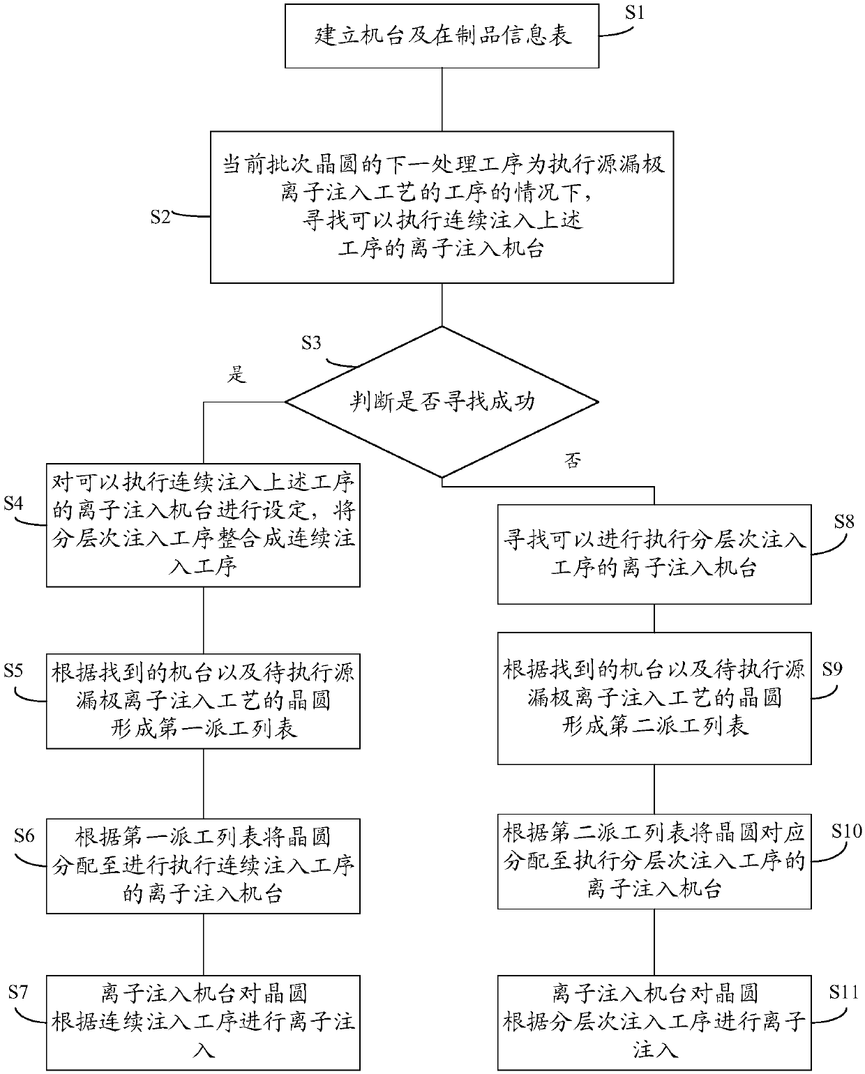
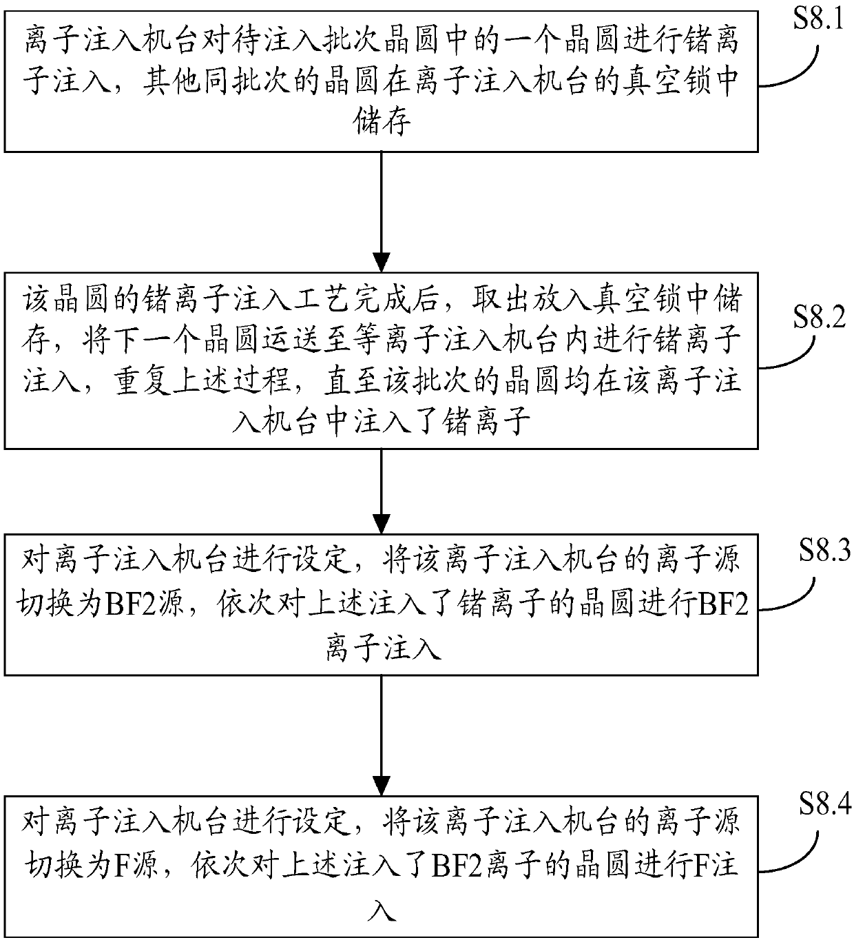
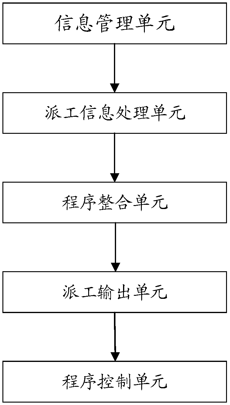
[0034] The invention will be described in more detail below with reference to the accompanying drawings, which show a preferred embodiment of the invention, it being understood that those skilled in the art can modify the invention described herein and still achieve the advantageous effects of the invention. Therefore, the following description should be understood as the broad knowledge of those skilled in the art, but not as a limitation of the present invention.

[0035] In the interest of clarity, not all features of an actual embodiment are described. In the following description, well-known functions and constructions are not described in detail since they would obscure the invention with unnecessary detail. It should be appreciated that in the development of any actual embodiment, numerous implementation details must be worked out to achieve the developer's specific goals, such as changing from one embodiment to another in accordance with system-related or business-rela...


PUM


Abstract

The invention discloses a source-drain ion implantation method and system. The method comprises the steps of: establishing a machine and a work-in-process information table; searching ion implantationmachines capable of performing source-drain ion implantation for a wafer by employing a continuous implantation process in a condition that the next processing process of the current batch of wafersis a process of executing source-drain ion implantation; setting the found ion implantation machines, and integrating the layered implantation processes into continuous implantation process; accordingto the found ion implantation machines and the wafers to be subjected to the source-drain ion implantation process, forming a first dispatch list; according to the first dispatch list, correspondingly distributing the wafers to the ion implantation machines; and performing source-drain ion implantation of the wafers according to the continuous implantation process by the ion implantation machines. The above-mentioned ion implantation process for forming an N-well is completed in the same ion implantation machine to achieve continuous source-drain implantation, reduce generation of wafer defects and reduce yield loss.

Description

technical field [0001] The invention relates to the field of integrated circuit manufacturing, in particular to a source-drain ion implantation method and an implantation system. Background technique [0002] The manufacturing process of semiconductors involves hundreds of detailed and complex processes, which must be skillfully coordinated according to strict manufacturing schedules. The semiconductor manufacturing process may include photolithography process, etching process, deposition process, polishing process, rapid thermal treatment process, implantation process, annealing process and so on. Thus, specialized equipment is required to perform the above-mentioned various processes according to well-defined manufacturing rules. [0003] With the scale of semiconductor production, the requirements for automation are getting higher and higher, and the Manufacturing Execution System (MES) has emerged as the times require. MES is a management system software used to track ...

Claims


Application Information

Patent Timeline
Patent Type & Authority Applications(China)
IPC IPC(8): H01L21/265H01L21/67
CPCH01L21/26506H01L21/26513H01L21/67276Y02P80/30
Inventor 李勇董卫一鸣
Owner SHANGHAI HUALI MICROELECTRONICS CORP
Why Eureka
Try Eureka