A method to solve the problem that high light transmittance wafer cannot be identified in lithography alignment

A high transmittance, unidentifiable technology, applied in electrical components, circuits, semiconductor/solid-state device manufacturing, etc., can solve the problems of low cost, high transmittance wafers cannot be identified, etc. simple craftsmanship

Active Publication Date: 2020-11-20
HUNAN SANAN SEMICON CO LTD
View PDF7 Cites 0 Cited by
  • Summary
  • Abstract
  • Description
  • Claims
  • Application Information

AI Technical Summary

Problems solved by technology

[0005] The purpose of the present invention is to overcome the deficiencies in the prior art, and provide a low-cost method for solving the problem that high-transmittance wafers cannot be identified in lithography alignment, and can simply and effectively unmatch the lithography machine in a short time. The wafers are transferred to the exposure station to complete a critical photolithography process

Method used


Image

  • A method to solve the problem that high light transmittance wafer cannot be identified in lithography alignment
  • A method to solve the problem that high light transmittance wafer cannot be identified in lithography alignment

Examples


Embodiment 1

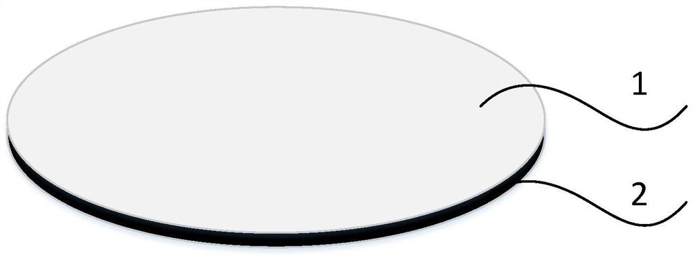
[0026] Step 1: If figure 1 As shown, before the photolithographic coating, low-cost processes such as sputtering, evaporation, physical vapor deposition or chemical vapor deposition are used to deposit carbon on the back of a high-transmittance wafer 1—such as a SiC wafer. A layer of low light transmittance film 2. The thickness of the carbon film is between 0.05 μm and 0.08 μm. The back side of the SiC wafer mentioned here specifically refers to the side that does not print graphics.

[0027] Step 2: Carry out conventional photolithography processes such as gluing, pre-baking, exposure, development, film hardening, corrosion, and degumming.

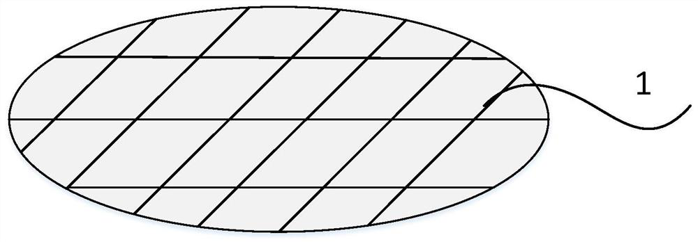
[0028] Step 3: After the entire photolithography process, use Descum O 2 removal of carbon film, such as figure 2 shown.

Embodiment 2

[0030] Step 1: Before photolithography coating, use low-cost processes such as sputtering, evaporation, physical vapor deposition or chemical vapor deposition to deposit TiW on the back of a high-transmittance wafer, such as a SiC wafer, to form a layer of low light transmittance film (2). The thickness of the TiW film is between 0.1 μm and 0.5 μm.

[0031] Step 2: Carry out conventional photolithography processes such as gluing, pre-baking, exposure, development, film hardening, corrosion, and degumming.

[0032] Step 3: After the entire photolithography process is completed, the TiW film is removed by soaking in SPM for 5-30 minutes.


PUM

PropertyMeasurementUnit
thicknessaaaaaaaaaa
thicknessaaaaaaaaaa

Abstract

The invention discloses a method for solving the problem that a high transmittance wafer cannot be recognized in photolithography alignment. A low transmittance film is formed at the back surface of ahigh transmittance wafer to perform a conventional photolithography process and remove the low transmittance film. The method can significantly reduce the light transmittance and can transfer the high transmittance wafer to the exposure stage to complete a critical lithography process. The method has low cost, high efficiency and a simple process, does not affect the quality of the wafer, does not affect the developer with each other, is not affected by the pre-bake and the film temperature, does not pollute the machine and is easy to remove the film, so that the method is an economical and simple method with high universality.

Description

technical field [0001] The invention belongs to the field of chip manufacturing, and in particular relates to a method for solving the problem that a wafer with high light transmittance cannot be identified during photolithographic alignment. Background technique [0002] Photolithography is one of the key technologies in the semiconductor chip manufacturing process. Exposure is a very important link in the photolithography process. Before the wafer starts to be exposed, there are 4 alignment steps: 1. Fine Retical Alignment; 2. Mechanical Pre-alignment; 3. TV Pre-alignment ); 4, Advanced Global Alignment (Advanced Globle Alignment); wherein, the mechanical pre-alignment is the rough alignment of the wafer before it is sent to the exposure platform, looking for the wafer gap and calculating the center position of the wafer, so that it can be accurately sent to the exposure station. [0003] Specifically, the mechanical pre-alignment unit analyzes the edge position of the ...

Claims


Application Information

Patent Timeline
Patent Type & Authority Patents(China)
IPC IPC(8): H01L21/027H01L21/67H01L21/68
CPCH01L21/0274H01L21/67294H01L21/68
Inventor 陶永洪高秀秀高建宁蔡文必
Owner HUNAN SANAN SEMICON CO LTD
Why Eureka
Try Eureka