
Application of gold nanometer bipyramids in OLED device

A gold nanometer and device technology is applied in the application field of gold nanobipyramid in OLED devices, which can solve the problems of no application and achieve the effect of improving performance and accelerating the process of excited and radiation transition.

Active Publication Date: 2019-03-29
NORTHEAST GASOLINEEUM UNIV
View PDF18 Cites 1 Cited by
  • Summary
  • Abstract
  • Description
  • Claims
  • Application Information

AI Technical Summary

Problems solved by technology

[0003] At present, spherical gold, silver, copper and other nanoparticles have been proven to improve the performance of OLED devices, while biconical gold nanoparticles are used in biosensing, photocatalysis, fluorescent probes, and surface-enhanced Raman scattering spectroscopy. and quantum dot solar cells and other fields, but the application in OLED has not been reported

Method used


Image

  • Application of gold nanometer bipyramids in OLED device
  • Application of gold nanometer bipyramids in OLED device
  • Application of gold nanometer bipyramids in OLED device

Examples


Embodiment 1

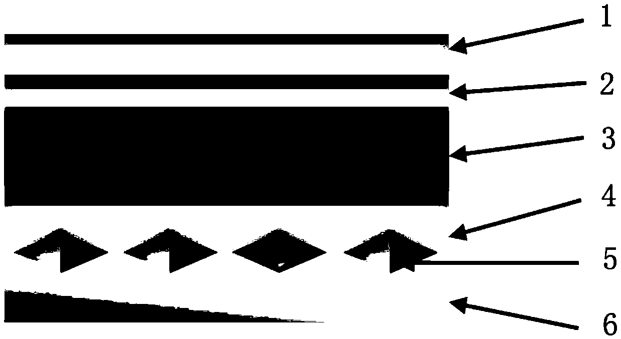
[0033] A gold nano bicone hybrid organic light-emitting diode device, including conductive glass ITO, gold nano bicone, zinc oxide, red light material MEH-PPV, molybdenum oxide layer and metal silver electrode, its preparation process is as follows:

[0034] (1) First, deposit a layer of gold nanobicones on the conductive glass (ITO) by electrostatic adsorption self-assembly method;

[0035] (2) A thin layer of zinc oxide was prepared as an electron transport layer by spin coating, and the distance between the gold nanobicones and the red light material was 6nm;

[0036] (3) Then spin-coat a layer of luminescent material with a thickness of 70nm;

[0037] (4) Finally, molybdenum oxide and metal silver electrodes are prepared by vapor deposition to obtain products.

Embodiment 2

[0039] A gold nano bicone hybrid organic light-emitting diode device, including conductive glass ITO, gold nano bicone, zinc oxide, red light material MEH-PPV, molybdenum oxide layer and metal silver electrode, its preparation process is as follows:

[0040] (1) First, deposit a layer of gold nanobicones on the conductive glass (ITO) by electrostatic adsorption self-assembly method;

[0041] (2) A thin layer of zinc oxide was prepared as an electron transport layer by spin coating, and the distance between the gold nanobicones and the luminescent material was 9nm;

[0042] (3) Then spin-coat a layer of luminescent material with a thickness of 85nm;

[0043] (4) Finally, molybdenum oxide and metal silver electrodes are prepared by vapor deposition to obtain products.

Embodiment 3

[0045] A gold nano bicone hybrid organic light-emitting diode device, including conductive glass ITO, gold nano bicone, zinc oxide, red light material MEH-PPV, molybdenum oxide layer and metal silver electrode, its preparation process is as follows:

[0046] (1) First, deposit a layer of gold nanobicones on the conductive glass (ITO) by electrostatic adsorption self-assembly method;

[0047] (2) A thin layer of zinc oxide was prepared as an electron transport layer by spin coating, and the distance between the gold nanobicones and the luminescent material was 12nm;

[0048] (3) Then spin-coat a layer of luminescent material with a thickness of 100nm;

[0049] (4) Finally, molybdenum oxide and metal silver electrodes are prepared by vapor deposition to obtain products.


PUM

PropertyMeasurementUnit
thicknessaaaaaaaaaa
diameteraaaaaaaaaa

Abstract

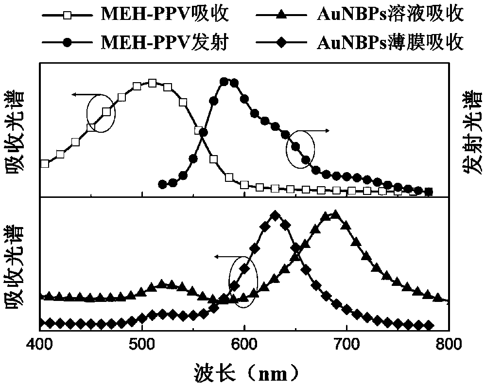
The invention discloses an application of gold nanometer bipyramids in an OLED device and further relates to a gold nano bipyramidal hybrid OLED device and a preparation method of the device. The method is advantaged in that through utilizing the surface plasmon resonance effect of the gold nanometer bipyramids, excitation and radiation transition of electrons are greatly accelerated, through adjusting the aspect ratio of the gold nanometer bipyramids, a surface plasmon resonance absorption band and absorption and emission spectra of luminescent materials are made to overlap to achieve the purpose of maximizing performance of the OLED device, and the gold nanometer bipyramids can generate a stronger electromagnetic field, the brightness and lumen efficiency of the gold nanometer bipyramidshybrid device are 2.22 times and 1.95 times the brightness and lumen efficiency of an original device, and performance of the OLED device is effectively improved.

Description

technical field [0001] The invention relates to the technical field of organic light-emitting diodes, in particular to the application of gold nano-bicones in OLED devices. Background technique [0002] Organic light-emitting diode (OLED) is an active light-emitting device that is expected to replace liquid crystal displays at present. It has the advantages of low operating voltage, high brightness, flexibility and bendability, and wide viewing angle. Its usual structure is composed of positive / negative electrodes, empty It is composed of a hole / electron transport layer and an organic light-emitting layer. The working principle of the device is that holes and electrons are injected from the positive and negative electrodes respectively, pass through the hole and electron transport layers respectively, and recombine and emit light in the light-emitting layer. Under light excitation, metal nanoparticles have surface plasmon resonance effect, which can improve the brightness an...

Claims


Application Information

Patent Timeline
Patent Type & Authority Applications(China)
IPC IPC(8): H01L51/50H01L51/56B82Y30/00
CPCB82Y30/00H10K50/00H10K71/00
Inventor 王欢赵阳张彪陈曦
Owner NORTHEAST GASOLINEEUM UNIV
Learn More