Low-pressure electroosmosis pump based on nano porous thin film
A nanoporous, porous film technology, used in laboratory containers, laboratory utensils, fluid controllers, etc., to achieve low cost, uniform pore size, and excellent mechanical effects
- Summary
- Abstract
- Description
- Claims
- Application Information
AI Technical Summary
Problems solved by technology
Method used
Image
Examples
Embodiment 1
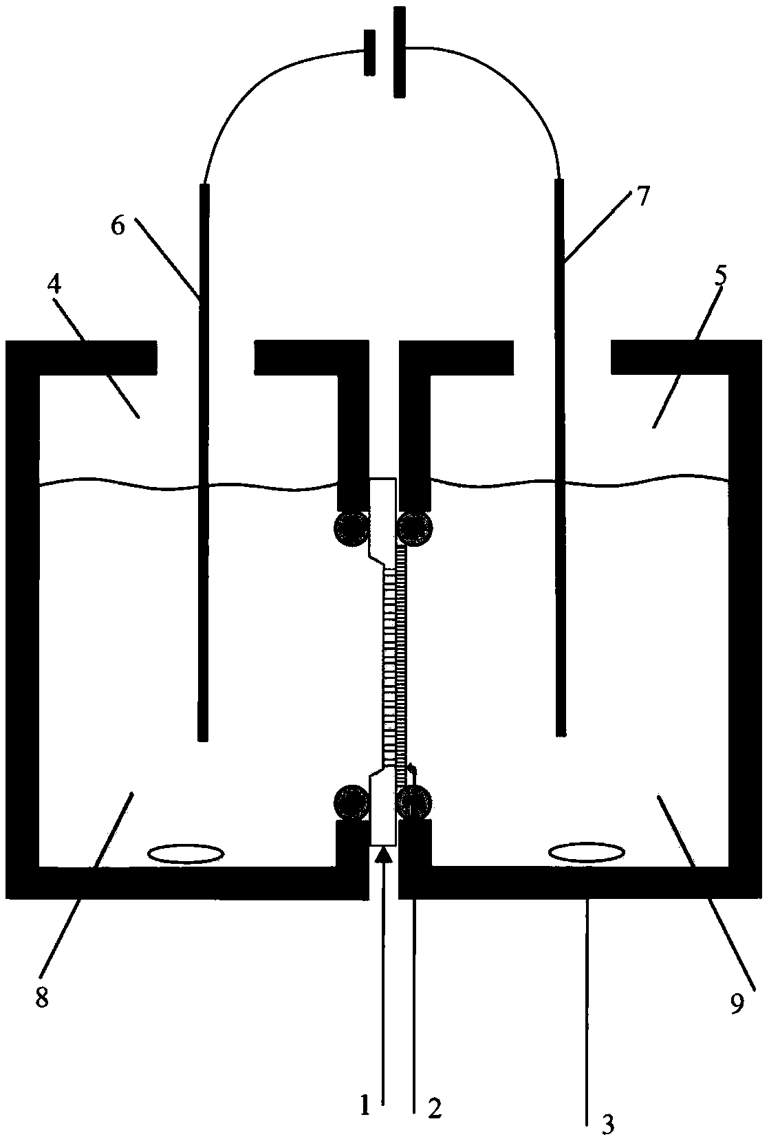
[0036] The structure of the low-voltage electroosmotic pump based on the nanoporous membrane is as follows: figure 1 As shown: the nanoporous film composed of nanoporous silicon dioxide film 2 and silicon nitride microporous film 1 forms a sandwich structure with two silica gel gaskets, and is integrated between the first chamber 4 and the second chamber 5; In the first chamber and the second chamber, silver / silver chloride electrodes are respectively installed as the first driving electrode 6 and the second driving electrode 7; the first chamber and the second chamber are filled with electrolyte solutions 8 and 9 .
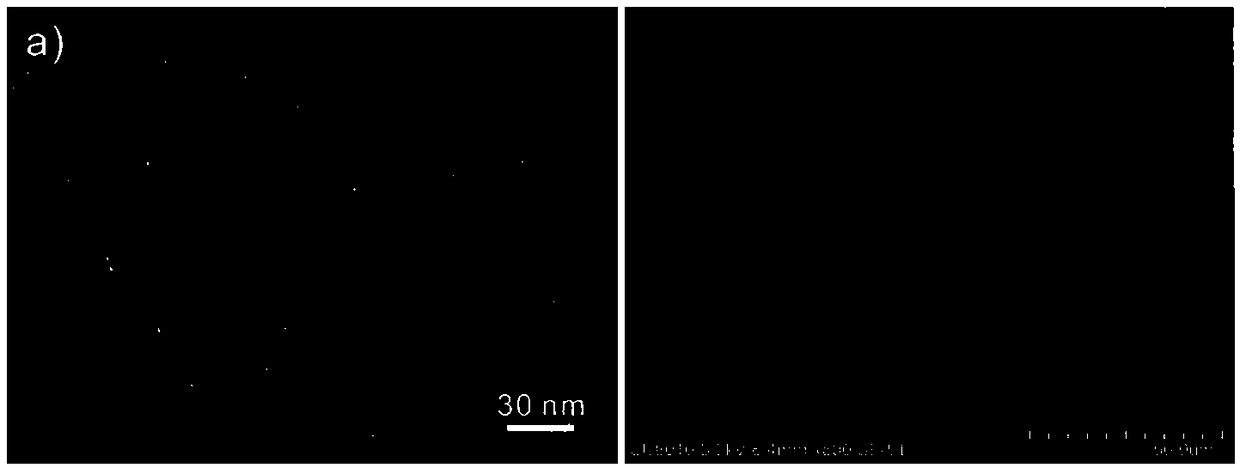
[0037] Transmission electron microscope image of nanoporous silica film figure 2 As shown, the scanning electron microscope image of the nanoporous film is shown in figure 2 shown. Among them, the average pore diameter of the nanoporous silicon dioxide film is 2.3nm, the porosity is 16.7%, and the thickness is 75nm; the thickness of the silicon nitride micro...
Embodiment 2
[0043] For the low-voltage electroosmotic pump provided in Example 1, the distance between the first driving electrode and the second driving electrode is 2mm; the average pore diameter of the nanoporous silicon dioxide film is 2nm, the porosity is 17%, and the thickness is 100nm; The silicon nitride microporous film has a thickness of 100 nm, a pore diameter of 4 μm, and a pore spacing of 40 μm.
Embodiment 3
[0045] For the low-voltage electroosmotic pump provided in Example 1, the distance between the first driving electrode and the second driving electrode is 2mm; the average aperture of the nanoporous silicon dioxide film is 2.5nm, the porosity is 16%, and the thickness is 100nm; The silicon microporous film has a thickness of 150 nm, a pore diameter of 6 μm, and a pore spacing of 20 μm.
PUM
| Property | Measurement | Unit |
|---|---|---|
| thickness | aaaaa | aaaaa |
| pore size | aaaaa | aaaaa |
| thickness | aaaaa | aaaaa |
Abstract
Description
Claims
Application Information
 - R&D
- Intellectual Property
- Life Sciences
- Materials
- Tech Scout
- Unparalleled Data Quality
- Higher Quality Content
- 60% Fewer Hallucinations
Browse by: Latest US Patents, China's latest patents, Technical Efficacy Thesaurus, Application Domain, Technology Topic, Popular Technical Reports.
© 2025 PatSnap. All rights reserved.Legal|Privacy policy|Modern Slavery Act Transparency Statement|Sitemap|About US| Contact US: help@patsnap.com


