
FPGA-based mapping-oriented network-on-chip verification method and system

An on-chip network and verification method technology, which is applied in the field of mapping-oriented network-on-chip verification, can solve the problems of lack of mapping power consumption, slow speed, lack of application-oriented mapping NoC verification platform, etc., and achieve the effect of fast simulation evaluation

Active Publication Date: 2019-03-08
UNIV OF ELECTRONICS SCI & TECH OF CHINA
View PDF4 Cites 6 Cited by
  • Summary
  • Abstract
  • Description
  • Claims
  • Application Information

AI Technical Summary

Problems solved by technology

The existing mapping verification platform has the following problems in the face of future application requirements: 1. Most of the existing NoC simulators are software simulation platforms written based on high-level programming languages, which have the disadvantage of slow speed when facing large-scale NoC simulation
The Booksim software emulator only needs a few simple C codes to realize the source data sending feature, but the clock frequency of the data packet sending module corresponding to the hardware requirements is much higher than the system clock, which does not conform to the real hardware situation
2. The proposed hardware verification platform is mainly aimed at the design and verification of NoC topology architecture, and lacks a NoC verification platform for application mapping
The verification platform of the appeal is limited to the simulation of the network-on-chip architecture, lacks the key simulation for the data characteristics of the application, and is limited to the simulation of network communication, so it cannot combine the content of multi-core processing to restore the working environment of the multi-core system; common hardware emulators The router is designed as a one-stage single-stage form, rather than the current multi-stage pipeline form. It does not support task mapping assignment in the multi-core field, and lacks power consumption and network congestion simulation data related to mapping.

Method used


Image

  • FPGA-based mapping-oriented network-on-chip verification method and system
  • FPGA-based mapping-oriented network-on-chip verification method and system
  • FPGA-based mapping-oriented network-on-chip verification method and system

Examples


Embodiment Construction

[0029] In the following, the present invention will be further described in detail in conjunction with the accompanying drawings and embodiments, so as to make the purpose, technical solutions and advantages of the present invention more clear. It should be understood that the specific embodiments described here are only used to explain the present invention, not to limit the present invention.

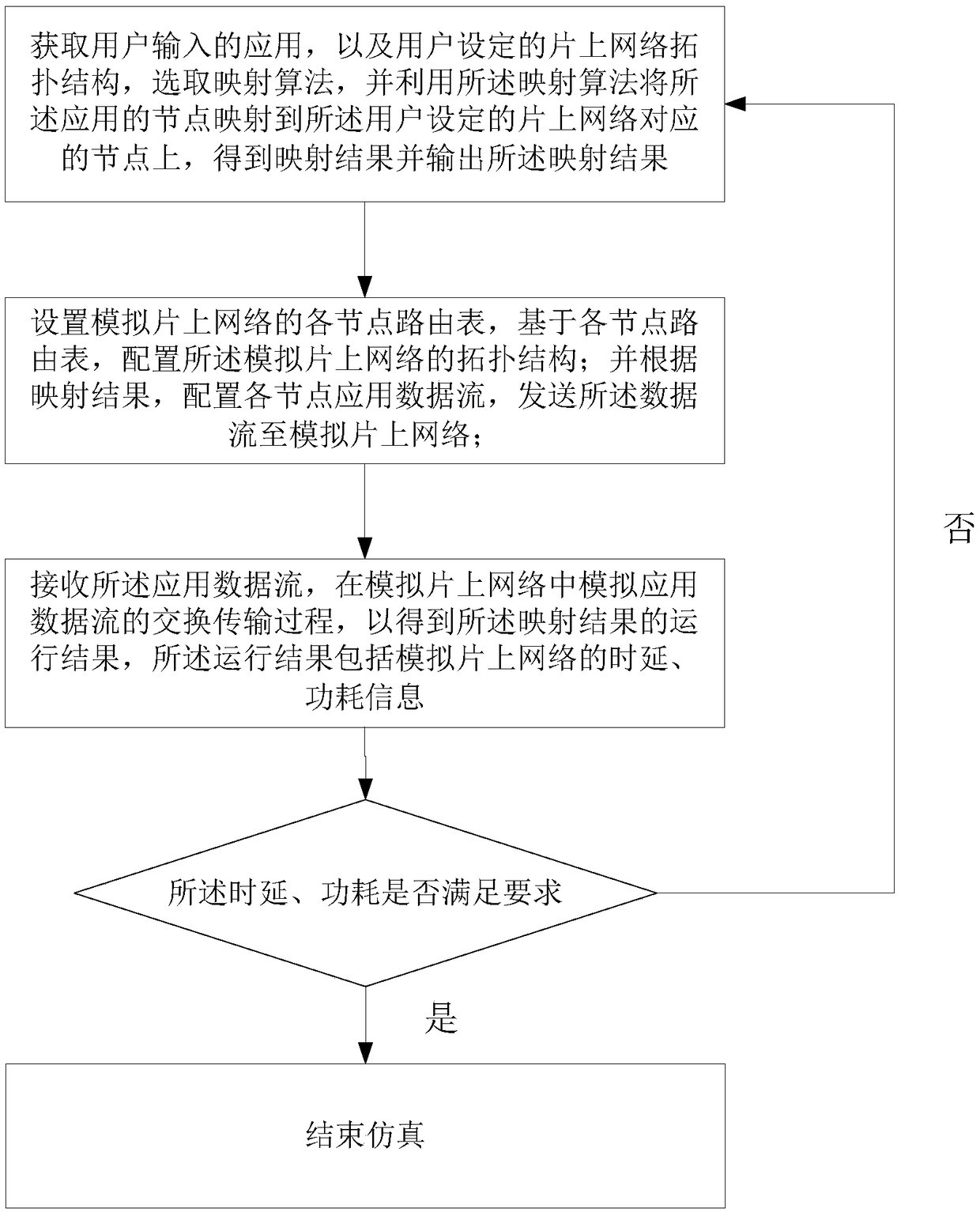
[0030] figure 1 A map-oriented network-on-chip verification method according to an exemplary embodiment of the present invention is shown. The method of this embodiment mainly includes:

[0031] S101: Obtain the application input by the user and the topology structure of the network on chip set by the user, select a mapping algorithm, and use the mapping algorithm to map the nodes of the application to the nodes corresponding to the network on chip set by the user, and obtain mapping the result and outputting the mapping result;

[0032] S102: Set the routing table of each node of ...


PUM


Abstract

The invention discloses an FPGA-based mapping-oriented network-on-chip verification method and system. The system introduces a mapping-oriented processing platform for application tasks (the processing platform comprises three mapping-oriented soft cores) to simulate and generate data features of the application tasks; furthermore, an analog network-on-chip simulation platform-MAENoC is further designed; by writing mapping application data to each node of an analog network-on-chip, an operation result of a mapping algorithm on the network-on-chip is monitored on line so as to realize rapid simulation and evaluation of an application mapping-oriented network-on-chip; the analog network-on-chip simulation platform-MAENoC is connected in the form of partitioning, and nodes in an area are connected by a bus; by use of a routing table configuration method, the system can simulate different topologies for generating NoC; each node supports dynamic reconstruction of multiple pipelined mechanisms and virtual channels; and meanwhile, a virtualization technology is added to support verification of an NoC with a large number of nodes.

Description

technical field [0001] The invention relates to the technical field of on-chip network verification, in particular to an FPGA-based mapping-oriented on-chip network verification method and system. Background technique [0002] With the development of artificial intelligence, machine learning / deep learning processors represented by GPU and general-purpose SoC have encountered problems such as long processing time and limited computing resources. Among the indicators in future 5G communications, processor design that requires multiple application scenarios, high concurrency, low power consumption, and "zero" delay brings higher challenges. On the other hand, according to the latest 7nm manufacturing process, 7 billion transistors can be integrated on a fingernail-sized chip. In deep sub-micron, the typical multicore processor system on chip based on the traditional bus design has bottlenecks such as limited bandwidth throughput, poor scalability, difficult global synchronizat...

Claims


Application Information

Patent Timeline
Patent Type & Authority Applications(China)
IPC IPC(8): H04L12/24H04L12/751H04L45/02
CPCH04L41/12H04L41/145H04L45/02
Inventor 徐志康陈亦欧凌翔
Owner UNIV OF ELECTRONICS SCI & TECH OF CHINA
Learn More