A light-emitting diode epitaxial wafer and its manufacturing method

A technology of light-emitting diodes and manufacturing methods, which is applied in the direction of semiconductor devices, electrical components, circuits, etc., can solve the problems of reducing efficiency and reducing luminous efficiency, and achieve the effects of large energy band gap, improving luminous efficiency, and reducing defects.

Active Publication Date: 2021-10-08
HC SEMITEK SUZHOU
View PDF7 Cites 0 Cited by
  • Summary
  • Abstract
  • Description
  • Claims
  • Application Information

AI Technical Summary

Problems solved by technology

[0005] Since the multi-quantum well layer is composed of InGaN quantum well layers and GaN quantum barrier layers alternately arranged in multiple periods, the InGaN quantum well layers and GaN quantum barrier layers will generate stress due to lattice mismatch. The period of the layer continues to increase, and the stress between the quantum well layer and the quantum barrier layer continues to accumulate. Some linear dislocations in the GaN epitaxial layer will develop and amplify during the quantum well growth process, forming V-shaped defects, thereby reducing the electron density. The efficiency of radiative recombination luminescence with holes in the multi-quantum well layer
At the same time, the InGaN quantum well layer and the GaN quantum barrier layer will produce a piezoelectric polarization effect due to lattice mismatch, resulting in the separation of the wave functions of electrons and holes in space, thereby reducing the luminous efficiency of LEDs.

Method used


Image

  • A light-emitting diode epitaxial wafer and its manufacturing method
  • A light-emitting diode epitaxial wafer and its manufacturing method

Examples


Embodiment Construction

[0027] In order to make the object, technical solution and advantages of the present invention clearer, the implementation manner of the present invention will be further described in detail below in conjunction with the accompanying drawings.

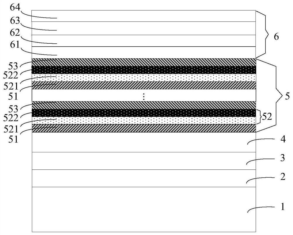
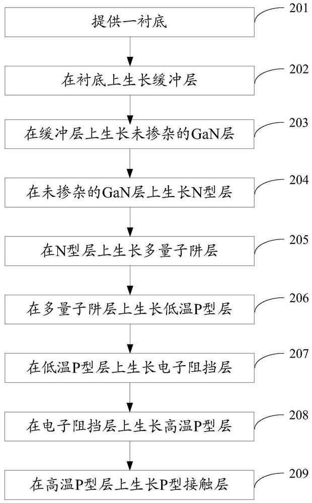
[0028] An embodiment of the present invention provides a light emitting diode epitaxial wafer, figure 1 It is a schematic structural diagram of a light-emitting diode epitaxial wafer provided by an embodiment of the present invention, as shown in figure 1 As shown, the light-emitting diode epitaxial wafer includes a substrate 1 , and a buffer layer 2 , an undoped GaN layer 3 , an N-type layer 4 , a multi-quantum well layer 5 and a P-type layer 6 stacked on the substrate 1 in sequence.

[0029] The multi-quantum well layer 5 is a multi-period superlattice structure, and each superlattice structure includes an InGaN quantum well layer 51, a transition layer 52 and a GaN quantum barrier layer 53 stacked on the InGaN quantum well layer 51 ...


PUM

PropertyMeasurementUnit
thicknessaaaaaaaaaa
thicknessaaaaaaaaaa
thicknessaaaaaaaaaa

Abstract

The invention discloses a light-emitting diode epitaxial wafer and a manufacturing method thereof, belonging to the technical field of semiconductors. The multi-quantum well layer of the light-emitting diode epitaxial wafer is a multi-period superlattice structure, and each superlattice structure includes an InGaN quantum well layer, a transition layer and a GaN quantum barrier layer stacked on the InGaN quantum well layer in sequence, and the transition layer It includes a first sublayer and a second sublayer arranged on the first sublayer, the first sublayer is an AlInN layer, and the second sublayer is an AlGaN layer. The lattice of AlInN material and InGaN material is relatively matched, the lattice of AlGaN material and GaN material is relatively matched, and the lattice of AlInN material and GaN material is also relatively matched, so the InGaN quantum can be reduced by setting the first sublayer and the second sublayer. The lattice mismatch between the well layer and the GaN quantum barrier layer reduces the generation of defects and improves the radiative recombination luminous efficiency of electrons and holes in the multi-quantum well layer.

Description

technical field [0001] The invention relates to the technical field of semiconductors, in particular to a light-emitting diode epitaxial wafer and a manufacturing method thereof. Background technique [0002] LED (Light Emitting Diode, Light Emitting Diode) is a semiconductor electronic component that can emit light. As an efficient, environmentally friendly and green new solid-state lighting source, it is being rapidly and widely used, such as traffic lights, car interior and exterior lights, urban landscape lighting, mobile phone backlights, etc. [0003] The epitaxial wafer is the main component of the LED. The existing GaN-based LED epitaxial wafer includes a substrate and a buffer layer stacked on the substrate in sequence, an undoped GaN layer, an N-type layer, a multi-quantum well layer and a P-type layer. Floor. The N-type layer is doped with Si to provide electrons, and the P-type layer is doped with Mg to provide holes. When the current is injected into the GaN-...

Claims


Application Information

Patent Timeline
Patent Type & Authority Patents(China)
IPC IPC(8): H01L33/06H01L33/32H01L33/00
CPCH01L33/0066H01L33/0075H01L33/06H01L33/325
Inventor 陶章峰乔楠张武斌余雪平程金连胡加辉
Owner HC SEMITEK SUZHOU
Why Eureka
Try Eureka