Thyristor and its manufacturing method

A thyristor and polysilicon layer technology, applied in the direction of thyristor, semiconductor/solid-state device manufacturing, semiconductor devices, etc., can solve the problems of increased power consumption of the circuit system, failure to work normally, long turn-off time, etc., to reduce conduction loss and enhance The effect of parameter stability and faster response speed

Active Publication Date: 2021-12-07
上海领矽半导体有限公司
View PDF7 Cites 0 Cited by
  • Summary
  • Abstract
  • Description
  • Claims
  • Application Information

AI Technical Summary

Problems solved by technology

[0003] With the development of power electronics technology, the technical indicators of thyristors include: forward voltage drop, reverse breakdown voltage and turn-off loss. At present, thyristors with traditional structures and processes often only have high reverse breakdown voltage. However, when the shutdown time is long, the loss in the shutdown process is large, which leads to an increase in the power consumption of the entire circuit system, and even cannot work normally at high frequencies.

Method used


Image

  • Thyristor and its manufacturing method
  • Thyristor and its manufacturing method
  • Thyristor and its manufacturing method

Examples


Embodiment Construction

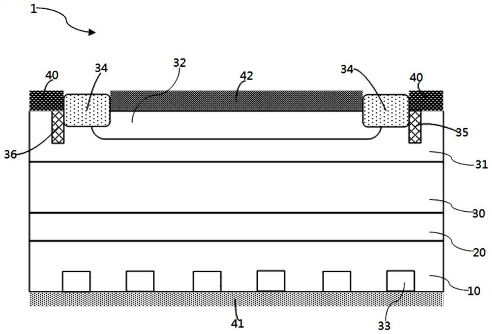
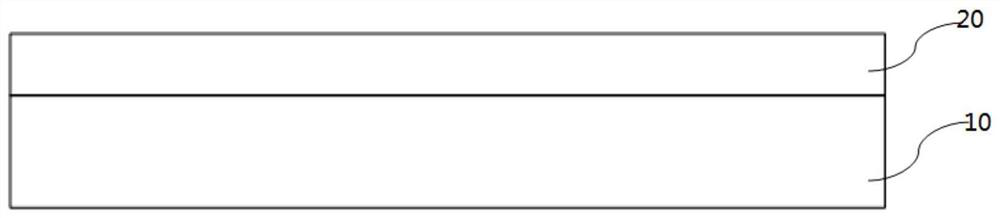
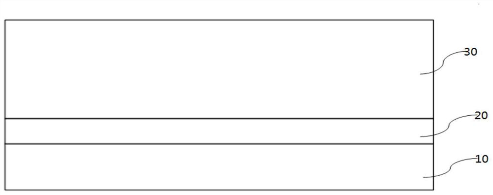
[0029] In order to understand the specific technical solutions, features and advantages of the present invention more clearly, the present invention will be further described in detail below in conjunction with the accompanying drawings and specific embodiments.

[0030] In the description of the present invention, it should be noted that the terms "upper", "lower", "left", "right", "transverse", "longitudinal", "horizontal", "inner", "outer" etc. indicate The orientation or positional relationship is based on the orientation or positional relationship shown in the drawings, or the orientation or positional relationship that is usually placed when the product of the invention is used, and is only for the convenience of describing the present invention and simplifying the description, rather than indicating or implying the It should not be construed as limiting the invention that a device or element must have a particular orientation, be constructed, and operate in a particular ...


PUM

PropertyMeasurementUnit
thicknessaaaaaaaaaa
thicknessaaaaaaaaaa
thicknessaaaaaaaaaa

Abstract

The present invention provides a thyristor comprising a substrate of the first conductivity type, a buried layer of the second conductivity type formed on the substrate, an epitaxial layer of the second conductivity type formed on the upper surface of the buried layer, and an epitaxial layer of the second conductivity type formed on the epitaxial layer A first implantation region of the first conductivity type on the upper surface, a second implantation region of the second conductivity type located in the first implantation region, extending from the lower surface of the substrate to a plurality of first conductivity type implants in the substrate at intervals The third implantation region, the oxide layer located at the junction between the first implantation region and the second implantation region, extends from the upper surface of the first implantation region to the first implantation region to open a trench located outside the oxide layer, The trench is filled with a polysilicon layer of the first conductivity type, a gate metal layer located on the first injection region and the upper surface of the polysilicon layer. The invention also provides a preparation method of the thyristor, which reduces the forward voltage drop and conduction loss of the thyristor, and improves the working efficiency and reliability of the thyristor.

Description

technical field [0001] The invention relates to the field of design and manufacture of semiconductor devices, in particular to a thyristor and a preparation method thereof. Background technique [0002] The thyristor is a three-terminal controllable switching device including PNPN four or more semiconductor layers. Its three terminals are the anode, cathode and gate respectively. By controlling the gate, the thyristor can be changed from the cut-off state to the conduction state. It can also change from the on state to the off state. It can control a large current with a small current, so that semiconductor devices can be extended from weak current to strong current. Therefore, thyristors are widely used in electronic circuits such as controllable rectification, AC voltage regulation, non-contact electronic switches, inverters and frequency conversion, and are typical devices for controlling large currents with small currents. [0003] With the development of power electro...

Claims


Application Information

Patent Timeline
Patent Type & Authority Patents(China)
IPC IPC(8): H01L29/74H01L29/06H01L21/332
CPCH01L29/0615H01L29/0684H01L29/66363H01L29/7424
Inventor 不公告发明人
Owner 上海领矽半导体有限公司
Why Eureka
Try Eureka