
A method for obtaining critical charge of single event upset of nanometer static random access memory

A single-particle flip, static random technology, used in instruments, electrical digital data processing, computing, etc.

Active Publication Date: 2019-03-08
NORTHWEST INST OF NUCLEAR TECH
View PDF3 Cites 5 Cited by
  • Summary
  • Abstract
  • Description
  • Claims
  • Application Information

AI Technical Summary

Problems solved by technology

[0007] To sum up, there are many problems in the timeliness, executability, and accuracy of the existing SRAM single-event flipping critical charge acquisition methods. On the other hand, the continuous improvement of spacecraft performance requirements for large-scale integrated Nano-devices are widely used. Therefore, it is of great practical significance to establish a new single-event flipping critical charge acquisition method suitable for nano-SRAM

Method used


Image

  • A method for obtaining critical charge of single event upset of nanometer static random access memory
  • A method for obtaining critical charge of single event upset of nanometer static random access memory
  • A method for obtaining critical charge of single event upset of nanometer static random access memory

Examples


Embodiment Construction

[0084] The present invention will be further described below in conjunction with the accompanying drawings and specific embodiments.

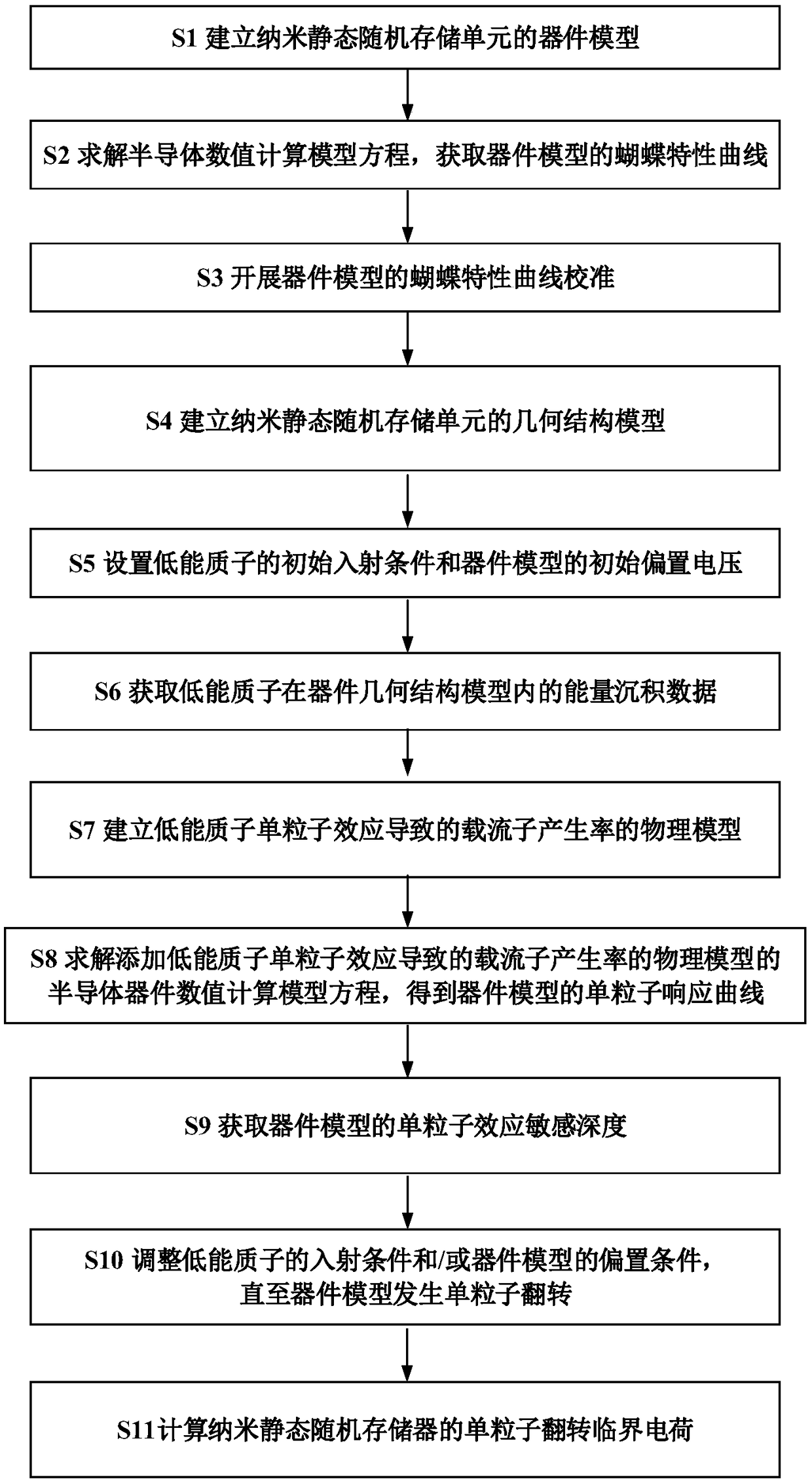
[0085] like figure 1 As shown, the method for obtaining the critical charge of single-event flipping in the nano-SRAM provided by the present invention includes the following steps:

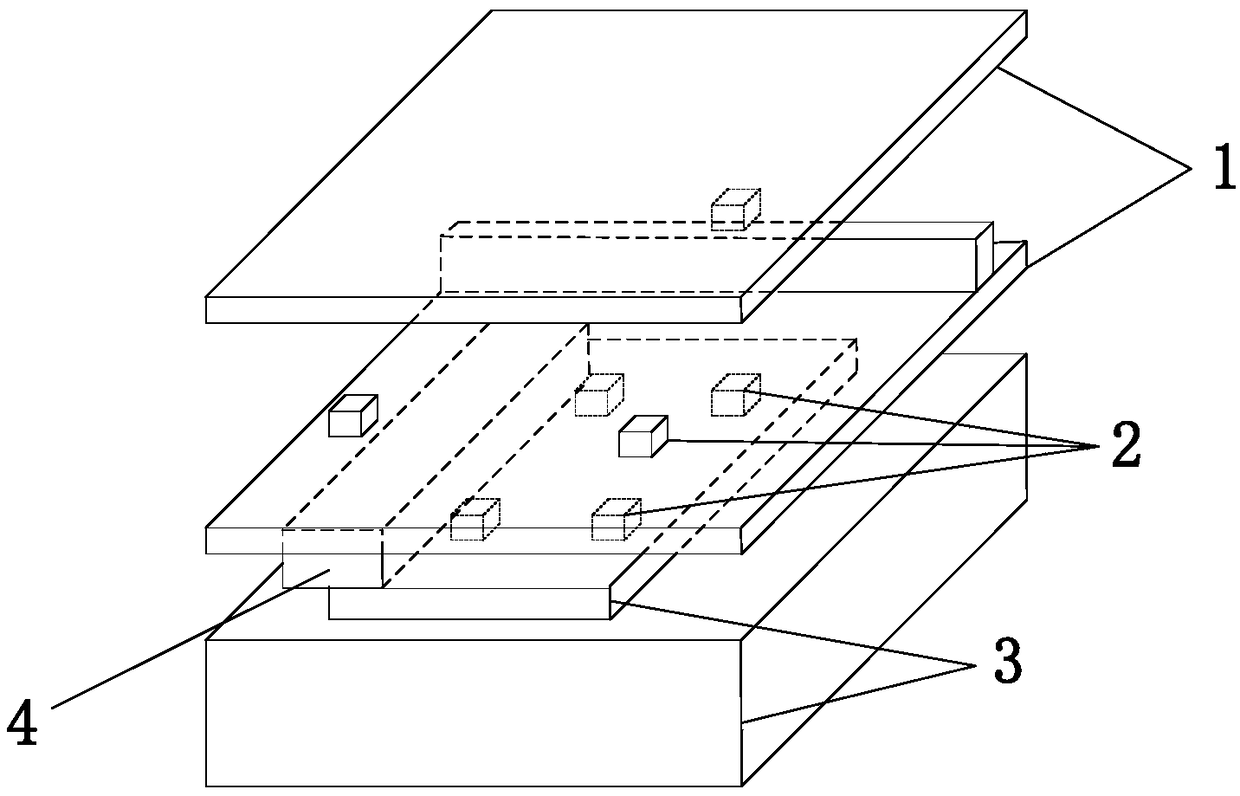
[0086] 1] Select the researched nano-SRAM, such as a certain type of SRAM, and obtain the material composition, geometric structure and doping parameters of the memory from the manufacturer of the SRAM (silicon dioxide 1, tungsten, titanium 2, silicon 3, aluminum 4), in TCAD, establish the device model of the SRAM through the device model editing language, such as figure 2 shown.

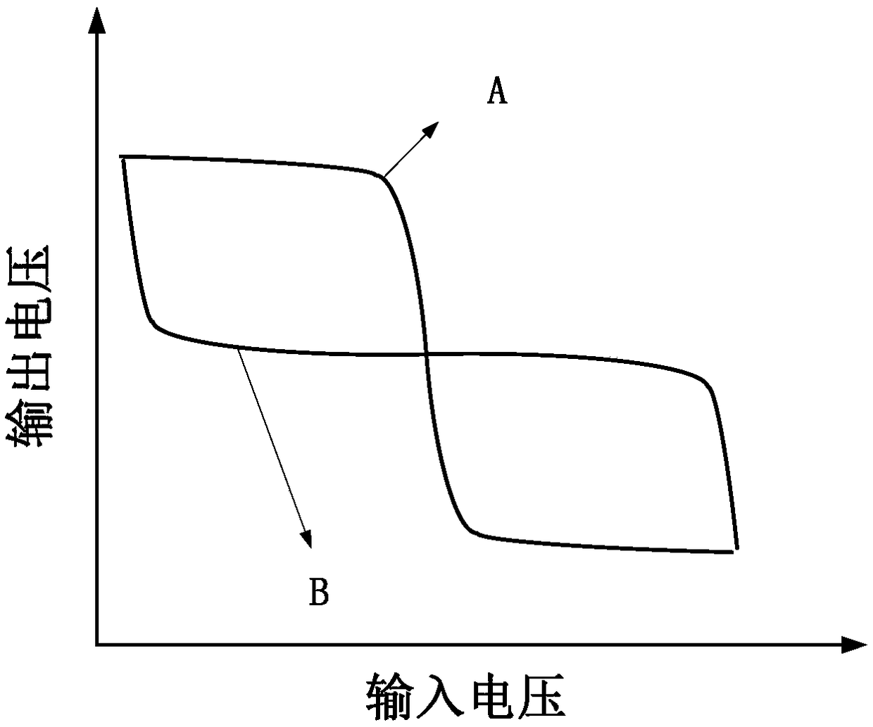
[0087] 2] Solve the numerical calculation model equations of semiconductor devices for the device model of SRAM, that is, the Poisson equation, the drift diffusion equation and the carrier continuity equation, and obtain the butterfly characteristic curve of the device model obtained...


PUM


Abstract

The invention provides a method for obtaining critical charge of single event upset of nanometer static random access memory based on simulation, which comprises the following steps of establishing adevice model of the nanometer static random access memory; obtaining the butterfly characteristic curve of the device model; calibrating the butterfly characteristic curve; constructing the geometricstructure model of static random access memory; setting initial incident conditions of low energy protons and initial bias voltage of device model; and obtaining the energy deposition data of low energy protons in the device geometry model; obtaining a physical model of carrier production rate caused by single event effect of low energy protons; obtaining the single particle response curve of thedevice model; obtaining the single event effect sensitivity depth of the device model; adjusting low-energy proton incident conditions and / or device model bias voltage until single event upset occursin the device model; and calculating the SEU critical charge of nano-SRAM. The method of the invention improves the obtaining efficiency of the critical charge of the single event upset, has low costand good executability.

Description

technical field [0001] The invention belongs to the technical field of space radiation effects and reinforcement, and relates to a simulation-based method for obtaining single-event flipping critical charge of a nano static random access memory. The nano-SRAM mentioned in the present invention refers to a SRAM whose characteristic process size is less than 100 nanometers. Background technique [0002] There are a large number of high-energy particles in the universe. The high-energy particles penetrate the shielding layer of the spacecraft and enter the internal electronic system and interact with the semiconductor devices in the system to generate charge deposition. The deposited charges are collected by sensitive circuit nodes in the system and cause the system to The function is damaged, affecting the reliable operation of the spacecraft in orbit. This effect is the result of the action of a single particle, so it is called a single event effect. [0003] The critical c...

Claims


Application Information

Patent Timeline
IPC IPC(8): G06F17/50
CPCG06F30/00
Inventor 赵雯陈伟王忠明郭晓强丛培天罗尹虹丁李利郭红霞潘霄宇王坦王勋
Owner NORTHWEST INST OF NUCLEAR TECH
Learn More