High-frequency electromagnetic wave shielding material
A shielding material and electromagnetic wave technology, which is applied in the fields of magnetic/electric field shielding, electrical components, film/sheet adhesives, etc., can solve the problems of difficult to take into account the electromagnetic shielding effect and poor high-frequency electromagnetic wave shielding effect, and achieve easy production The effect of preparation, excellent shielding performance, and high-efficiency electromagnetic shielding effect
- Summary
- Abstract
- Description
- Claims
- Application Information
AI Technical Summary
Problems solved by technology
Method used
Image
Examples
Embodiment 1
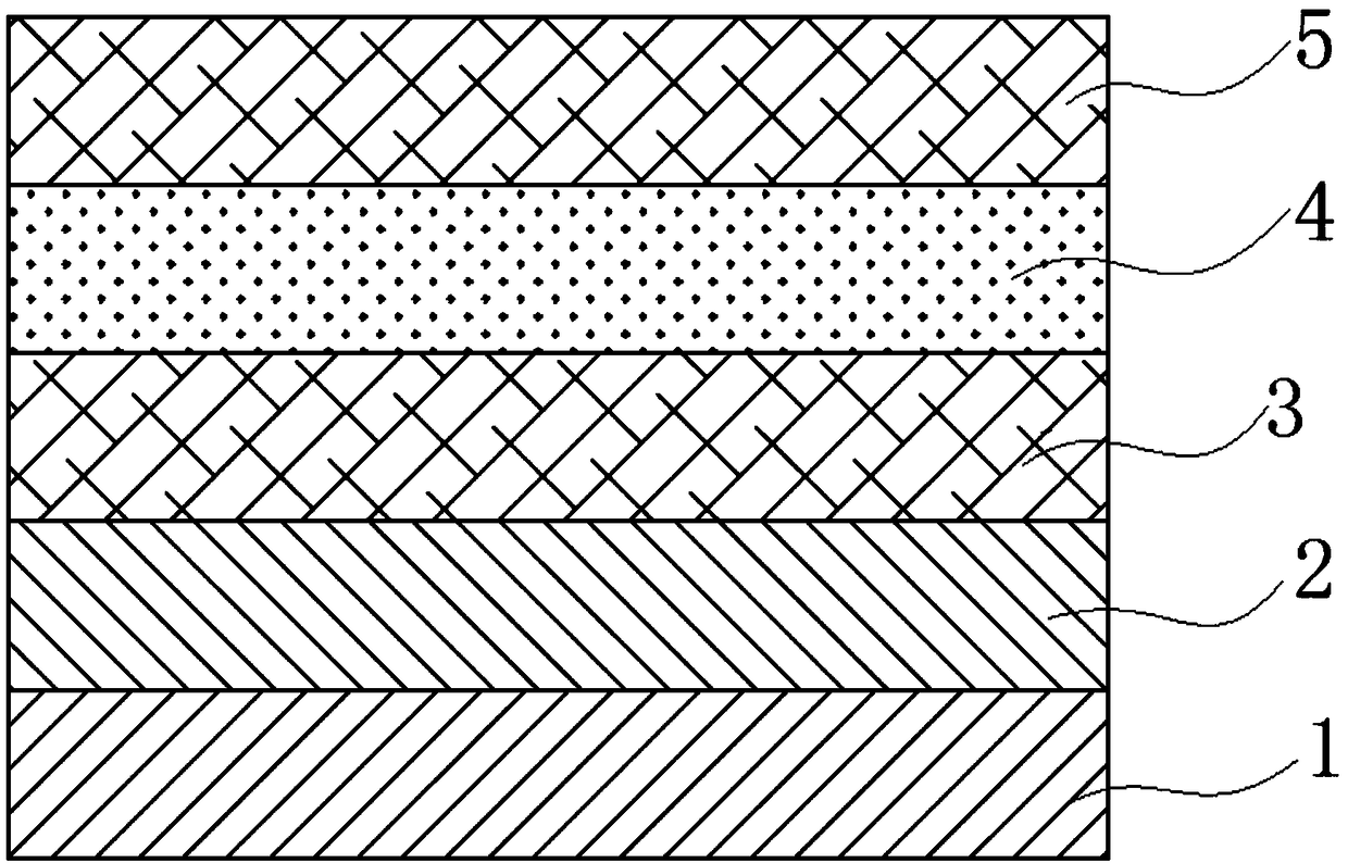
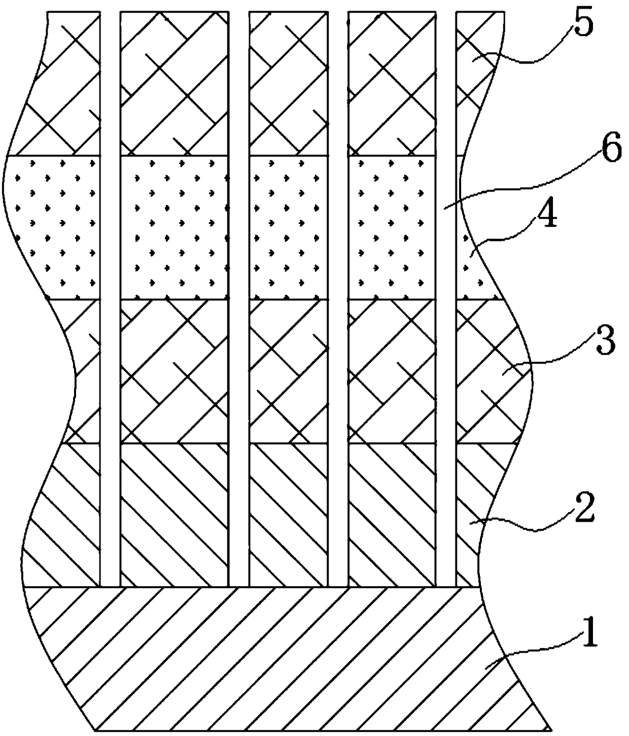
[0024] This embodiment provides a high-frequency electromagnetic wave shielding material, which can be used to shield electromagnetic radiation generated by electronic equipment. The electromagnetic shielding material is as follows: Figure 1-2 As shown, it consists of a release film layer 1 , an adhesive layer 2 , a first alloy layer 3 , a shielding base layer 4 and a second alloy layer 5 which are sequentially stacked and connected from bottom to top. The thickness of the shielding material is 0.02mm.
[0025] Wherein, the release film layer 1 is one of PE release film, PET release film, PC release film, and PMMA release film, and the material of the back adhesive layer 2 is acrylic or silica gel. , In this embodiment, the adhesive layer is made of acrylic glue. Both the first alloy layer 3 and the second alloy layer 5 are made of alloy materials of Ai, Si, Fe, Cu, Mn, Mg, Cr, Zn, Ti, and the first alloy layer 3 and the second alloy layer 5 evenly covers the upper and lowe...
Embodiment 2
[0028] This embodiment provides a high-frequency electromagnetic wave shielding material, which can be used to shield electromagnetic radiation generated by electronic equipment. The electromagnetic shielding material is as follows: Figure 1-2 As shown, it consists of a release film layer 1 , an adhesive layer 2 , a first alloy layer 3 , a shielding base layer 4 and a second alloy layer 5 which are sequentially stacked and connected from bottom to top. The thickness of the shielding material is 0.3 mm.
[0029] Wherein, the release film layer 1 is one of PE release film, PET release film, PC release film, and PMMA release film, and the material of the back adhesive layer 2 is acrylic or silica gel. , In this embodiment, the adhesive layer is made of acrylic glue. Both the first alloy layer 3 and the second alloy layer 5 are made of alloy materials of Ai, Si, Fe, Cu, Mn, Mg, Cr, Zn, Ti, and the first alloy layer 3 and the second alloy layer 5 evenly covers the upper and lowe...
Embodiment 3
[0032] This embodiment provides a high-frequency electromagnetic wave shielding material, which can be used to shield electromagnetic radiation generated by electronic equipment. The electromagnetic shielding material is as follows: Figure 1-2 As shown, it consists of a release film layer 1 , an adhesive layer 2 , a first alloy layer 3 , a shielding base layer 4 and a second alloy layer 5 which are sequentially stacked and connected from bottom to top. The thickness of the shielding material is 0.15mm.
[0033] Wherein, the release film layer 1 is one of PE release film, PET release film, PC release film, and PMMA release film, and the material of the back adhesive layer 2 is acrylic or silica gel. , In this embodiment, the adhesive layer is made of acrylic glue. Both the first alloy layer 3 and the second alloy layer 5 are made of alloy materials of Ai, Si, Fe, Cu, Mn, Mg, Cr, Zn, Ti, and the first alloy layer 3 and the second alloy layer 5 evenly covers the upper and lowe...
PUM
| Property | Measurement | Unit |
|---|---|---|
| Thickness | aaaaa | aaaaa |
| Thickness | aaaaa | aaaaa |
| Thickness | aaaaa | aaaaa |
Abstract
Description
Claims
Application Information
 - R&D
- Intellectual Property
- Life Sciences
- Materials
- Tech Scout
- Unparalleled Data Quality
- Higher Quality Content
- 60% Fewer Hallucinations
Browse by: Latest US Patents, China's latest patents, Technical Efficacy Thesaurus, Application Domain, Technology Topic, Popular Technical Reports.
© 2025 PatSnap. All rights reserved.Legal|Privacy policy|Modern Slavery Act Transparency Statement|Sitemap|About US| Contact US: help@patsnap.com


