A touch display panel and a manufacturing method thereof

A technology for a touch display panel and a manufacturing method, which are applied in the fields of instruments, electrical digital data processing, and data processing input/output processes, etc., can solve problems such as manufacturing interference, and achieve the effect of improving product yield.

Active Publication Date: 2019-03-01
WUHAN CHINA STAR OPTOELECTRONICS SEMICON DISPLAY TECH CO LTD
View PDF12 Cites 22 Cited by
  • Summary
  • Abstract
  • Description
  • Claims
  • Application Information

AI Technical Summary

Problems solved by technology

[0006] The present application provides a touch display panel and a manufacturing method to solve the technical problem that the organic light-emitting device in the existing touch display panel interferes with the preparation of the touch layer

Method used


Image

  • A touch display panel and a manufacturing method thereof
  • A touch display panel and a manufacturing method thereof
  • A touch display panel and a manufacturing method thereof

Examples


Embodiment Construction

[0049] The following descriptions of the various embodiments refer to the accompanying drawings to illustrate specific embodiments that the present application can be used to implement. The directional terms mentioned in this application, such as [top], [bottom], [front], [back], [left], [right], [inside], [outside], [side], etc., are for reference only The orientation of the attached schema. Therefore, the directional terms used are used to illustrate and understand the application, but not to limit the application. In the figures, structurally similar elements are denoted by the same reference numerals.

[0050] The present application provides a touch display panel and a manufacturing method to solve the technical problem that the organic light-emitting device in the existing touch display panel interferes with the preparation of the touch layer.

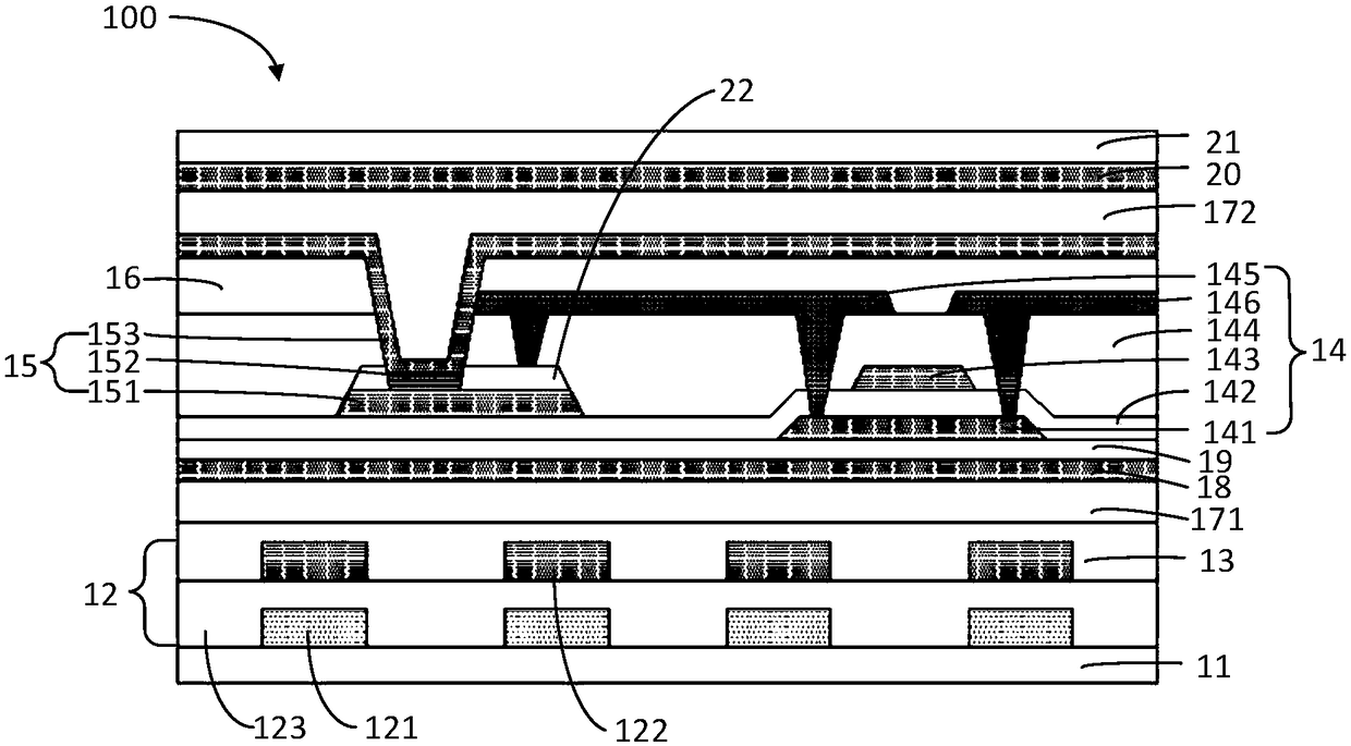
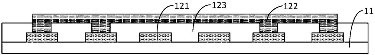
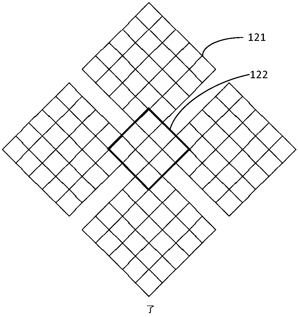
[0051] see figure 1 , figure 1 It is a cross-sectional view of the touch display panel 100 provided in the first embodiment...


PUM


Abstract

The invention provides a touch display panel and a manufacturing method. The touch display panel comprises a substrate, a touch layer, a protective layer, an array substrate and an organic light-emitting device. The touch layer comprises a touch pattern layer, a first insulating layer and a bridging layer. The organic light emitting device includes an anode, a cathode, and a light emitting layer disposed between the anode and the cathode. The touch layer is arranged between the substrate and the organic light-emitting device, and the touch layer is prepared first and then the organic light-emitting device is prepared, so that the process of the touch layer is not affected by the organic light-emitting device, and the product yield is improved.

Description

technical field [0001] The present application relates to the display field, in particular to a touch display panel and a manufacturing method thereof. Background technique [0002] With the development of the information age and the acceleration of the pace of life, touch technology has gradually replaced the traditional mouse and keyboard due to its humanized design and simple and fast input, and is widely used in various electronic products. Among them, Capacitive touch screens are widely used due to their fast response, high sensitivity, and good reliability. [0003] According to different configurations of the touch sensing layer in the display panel, the touch display panel is divided into structures such as Addon Mode, In-cell and On-cell. Considering factors such as process technology and yield rate, currently only mass production of display devices using on-cell technology can be realized. [0004] Because the organic light-emitting device in the touch display pa...

Claims


Application Information

Patent Timeline
IPC IPC(8): G06F3/041
CPCG06F3/0412G06F2203/04103
Inventor 冯校亮
Owner WUHAN CHINA STAR OPTOELECTRONICS SEMICON DISPLAY TECH CO LTD
Why Eureka
Try Eureka