Single-passband double-sided wave-absorbing metamaterial radome, application thereof and aircraft
A single passband and radome technology, applied in the field of radomes, can solve problems such as unfavorable components stealth, and achieve the effect of reducing RCS
- Summary
- Abstract
- Description
- Claims
- Application Information
AI Technical Summary
Problems solved by technology
Method used
Image
Examples
Embodiment 1
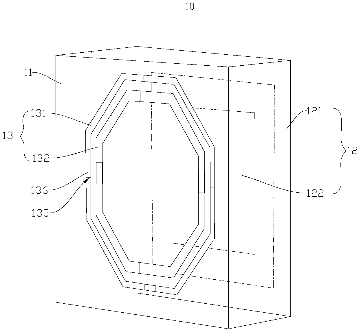
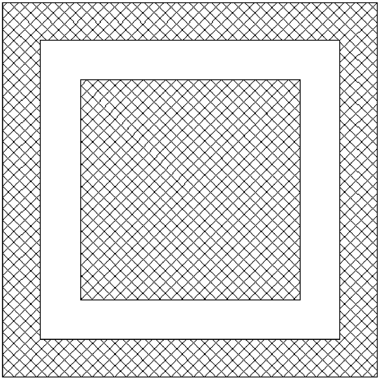
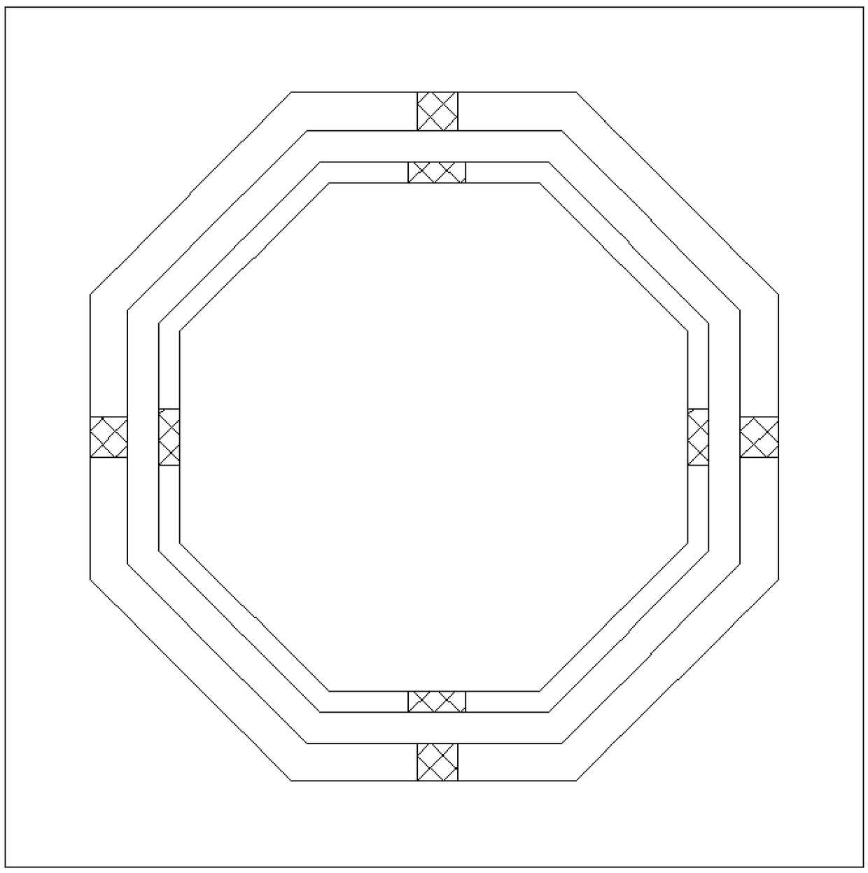
[0054] This embodiment provides a metamaterial radome 10 with single-pass band and double-sided absorbing, please refer to figure 1 and image 3 , the single-pass-band double-sided wave-absorbing metamaterial radome 10 includes a plurality of unit structures arranged sequentially in a square cycle, and each unit structure includes a dielectric layer 11 , a reflective layer 12 and a wave-absorbing layer 13 . The reflective layer 12 is arranged on one side of the medium layer 11, and the wave-absorbing layer 13 is set on the side of the medium layer 11 away from the reflective layer 12, and the reflective layer 12, the medium layer 11 and the wave-absorbing layer 13 are bonded by vinyl resin together to form a resonant cavity.
[0055] The dielectric layer 11 is made of polytetrafluoroethylene with a dielectric constant of 2.1 and a loss tangent of 0.0002, and the thickness of the dielectric layer 11 is 4.5 mm.
[0056] The reflective layer 12 is a copper reflective layer 12 w...
Embodiment 2
[0060] The difference between this embodiment and Embodiment 1 is that the dielectric layer is made of a low dielectric material with a dielectric constant of 2.0 and a loss tangent of 0.0001, and the thickness of the dielectric layer is 4.2 mm.
[0061] The reflective layer is a copper reflective layer with a total thickness of 0.08mm. The inner side length of the square ring located on the outside is 11mm, and the line width is 1.2mm; the side length of the square plate located on the inner side is 8mm.
[0062] The thickness of the wave-absorbing layer is 0.08 mm, the radius of the circumscribed circle of the outer octagonal ring is 6.2 mm, and the line width is 0.3 mm; the radius of the circumscribed circle of the inner octagonal ring is 5 mm, and the line width is 0.6 mm.
[0063] The length of the opening of the outer octagonal ring is 0.7 mm, and the length of the opening of the inner octagonal ring is 0.9 mm. Each opening is equipped with a 650-ohm chip resistor.
Embodiment 3
[0065] The difference between this embodiment and Embodiment 1 is that the dielectric layer is made of a low dielectric material with a dielectric constant of 2.2 and a loss tangent of 0.0003, and the thickness of the dielectric layer is 4.8 mm.
[0066] The reflective layer is a copper reflective layer with a total thickness of 0.1 mm. The inner side length of the square ring located on the outside is 11.5 mm, and the line width is 1.35 mm; the side length of the square plate located on the inner side is 8.8 mm.
[0067] The thickness of the wave-absorbing layer is 0.1 mm, the radius of the circumscribed circle of the outer octagonal ring is 6.8 mm, and the line width is 0.5 mm; the radius of the circumscribed circle of the inner octagonal ring is 5.4 mm, and the line width is 0.8 mm.
[0068] The length of the opening of the outer octagonal ring is 0.75 mm and the length of the opening of the inner octagonal ring is 0.95 mm. Each opening is equipped with a 750-ohm chip resis...
PUM
| Property | Measurement | Unit |
|---|---|---|
| Thickness | aaaaa | aaaaa |
| Line width | aaaaa | aaaaa |
| Thickness | aaaaa | aaaaa |
Abstract
Description
Claims
Application Information
 - Generate Ideas
- Intellectual Property
- Life Sciences
- Materials
- Tech Scout
- Unparalleled Data Quality
- Higher Quality Content
- 60% Fewer Hallucinations
Browse by: Latest US Patents, China's latest patents, Technical Efficacy Thesaurus, Application Domain, Technology Topic, Popular Technical Reports.
© 2025 PatSnap. All rights reserved.Legal|Privacy policy|Modern Slavery Act Transparency Statement|Sitemap|About US| Contact US: help@patsnap.com


