


Quick Research
Generate reliable direction feasibility study reports for your R&D in just a few steps.

Technical Q&A
Discover and master advanced knowledge NOW. Basics, ideas, possibilities, all at once.

Find Solutions
As an expert in R&D theories, this can generate solutions to your technical problems instantly.

Evaluate Feasibility
Analyze your overall solution with one click, know your potential R&D risks in advance.

Monitor Landscape
Get weekly tech updates, stay abreast of the latest tech innovations and key insights.
Translucent battery based on PLD growth inorganic CuGaO<2> transparent film
A transparent film and semi-transparent technology, applied in circuits, photovoltaic power generation, electrical components, etc., can solve problems such as high cost, low efficiency of organic solar cells, instability of dye-sensitized solar cells, etc., and achieve an optimized and stable structure, The effect of optimizing performance
- Summary
- Abstract
- Description
- Claims
- Application Information
AI Technical Summary
Problems solved by technology
Method used
Image

Examples
Embodiment 1
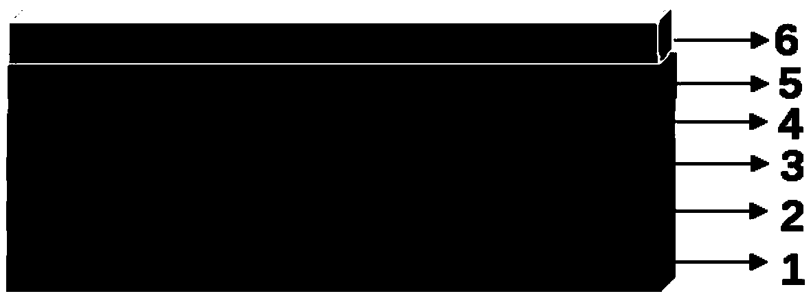
[0014] (1) Cut the FTO transparent conductive glass into 1.5cm long strips, then paste a 1cm wide tape, and then etch with zinc powder and concentrated hydrochloric acid and dilute hydrochloric acid with a volume ratio of 1:5 for 15 minutes, then use dilute hydrochloric acid Clean the residual zinc powder, cut the etched glass into 1.5×1.5cm squares, ultrasonically clean with lye for 30-60min, then ultrasonically clean with alcohol for 30-60min, and finally clean with deionized water for 10-30min, then Put it into a drying oven to dry to obtain the first transparent electrode substrate (as shown in Figure 1, layer 1);
[0015] (2) Utilize PLD to deposit CuGaO on the surface of the above-mentioned first transparent electrode substrate 2 Nanoparticles, the frequency is 5HZ, the energy is 300mJ, and CuGaO is deposited on the surface 2 The first transparent electrode substrate of the hole transport film (as shown in Figure 1, 2 layers);
[0016] (3) Dissolve lead iodide and cesi...
Embodiment 2
[0020] (1) The present embodiment is the same as Example 1, except that step (4) dissolves PCBM in chlorobenzene and stirs for twelve hours to obtain the PCBM precursor solution, the concentration is 20mg / ml, and then spin-coats CsPbI 3 The substrate surface of the thin film is spin-coated with PCBM precursor solution at a speed of 2000 rpm / s for 30 s to obtain a substrate coated with a PCBM electron transport thin film (as shown in Figure 1 with 4 layers); use a vacuum thermal evaporation coater to vapor-deposit ultra-thin Ag Electrode, thickness 10nm, evaporation rate is As a conductive layer (as shown in Figure 1, 5 layers), the light anti-reflection layer MoO is finally evaporated with a vacuum thermal evaporation coater. 3 (6 layers as shown in Figure 1), the thickness is 40nm, and the evaporation rate is Complete the preparation of semi-transparent perovskite solar cells.
Embodiment 3
[0022] (1) the present embodiment is the same as embodiment 1, the difference is that step (5) FeCl 3 Dissolve in ethylene glycol solution (10ml), continue to add polyvinylpyrrolidone (PVP), then move the solution to a stirring heater to heat at 80-100°C, stir for 5min for later use; 3 Dissolve in ethylene glycol solution (10ml), take out 15-20ul and add it dropwise to the standby solution, when the solution turns brown, remove the remaining AgNO 3 The solution is mixed in, then the solution is moved to the reaction kettle at 150-200°C for 2-3 hours, and finally the solution is centrifuged and ultrasonicated to obtain the silver nanowire precursor solution, and the silver nanowire precursor solution is spin-coated with a homogenizer at a speed of 3000-7000r / min, the time is 30-50s to make silver nanowire transparent electrode (as shown in Figure 1, 5 layers); use vacuum thermal evaporation coating device to vapor-deposit light anti-reflection layer MoO 3 (6 layers as shown i...
PUM
| Property | Measurement | Unit |
|---|---|---|
| Diameter | aaaaa | aaaaa |
| Thickness | aaaaa | aaaaa |
Abstract
Description
Claims
Application Information
 - R&D Engineer
- R&D Manager
- IP Professional
- Industry Leading Data Capabilities
- Powerful AI technology
- Patent DNA Extraction
Browse by: Latest US Patents, China's latest patents, Technical Efficacy Thesaurus, Application Domain, Technology Topic, Popular Technical Reports.
© 2024 PatSnap. All rights reserved.Legal|Privacy policy|Modern Slavery Act Transparency Statement|Sitemap|About US| Contact US: help@patsnap.com