Solder resist process method for improving solder resist ghost

A process method and solder mask technology, applied in the secondary processing of printed circuits, electrical components, printed circuit manufacturing, etc., to save production costs, reduce production cycles, and improve the effect of blocking point nets

Active Publication Date: 2019-01-25
DALIAN CHONGDA CIRCUIT
View PDF5 Cites 2 Cited by
  • Summary
  • Abstract
  • Description
  • Claims
  • Application Information

AI Technical Summary

Problems solved by technology

[0004] The purpose of the present invention is to overcome the above-mentioned defects in the prior art, and provide a solder resist process method for improving solder resist gh...

Method used


Image

  • Solder resist process method for improving solder resist ghost
  • Solder resist process method for improving solder resist ghost
  • Solder resist process method for improving solder resist ghost

Examples


Embodiment Construction

[0019] The specific embodiment of the present invention will be further described in detail below in conjunction with the accompanying drawings.

[0020] It should be noted that, in the following specific embodiments, when describing the embodiments of the present invention in detail, in order to clearly show the structure of the present invention for the convenience of description, the structures in the drawings are not drawn according to the general scale, and are drawn Partial magnification, deformation and simplification are included, therefore, it should be avoided to be interpreted as a limitation of the present invention.

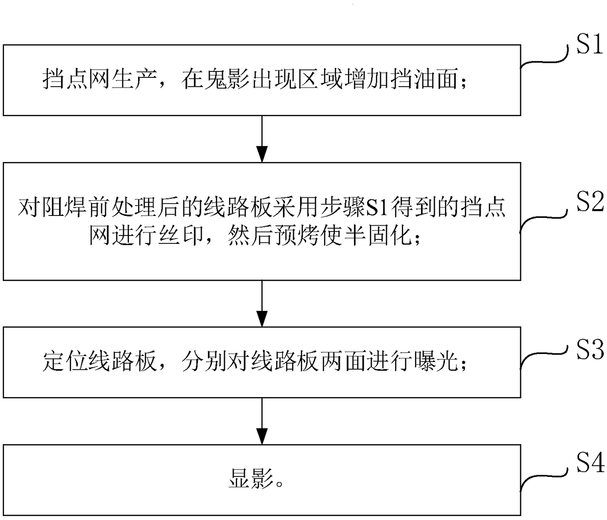
[0021] In the following specific embodiments of the present invention, please refer to figure 1 . As shown in the figure, the present invention discloses a solder resist process method for improving solder resist ghosting, which is characterized in that it includes the following steps:

[0022] Step S1: Production of the blocking point net, adding ...


PUM


Abstract

The invention discloses a welding resistance process method for improving the welding resistance ghost, which comprises the following steps: step S1, producing a stopping point net, adding an oil stopping surface in the region where the ghost appears; step S2, adding a oil stopping surface in the region where the ghost appears; step S1, adding an oil stopping surface in the region where the ghostappears. Step S2: The circuit board after the pre-treatment of solder resistance is screen-printed with the stop screen obtained in step S1, and then pre-roasted to make semi-solidified; 3, position that circuit board and exposing both side of the circuit board respectively; Step S4: Development. The invention has the advantages of reducing the production cycle and shortening the production process, which not only improves the quality problems such as ghost, oil dropping and bridge dropping, but also saves the production cost.

Description

technical field [0001] The invention relates to the field of printed circuit board manufacturing, and more particularly relates to a solder resist process method for improving solder resist ghost images. Background technique [0002] The sequence of the existing solder mask process is as follows: solder mask pretreatment → silk screen → pre-baking → alignment exposure → development → QC inspection → next solder mask process, specifically, during silk screen printing, silk screen printing is performed on both sides of the circuit board, and then pre-baking , to make the green oil semi-cured, or, for thin boards below 0.8mm, when silk-screening, one side of the circuit board should be screen-printed first, then pre-baked to make the green oil semi-cured, and then silk-screened on the other side of the circuit board, and then pre-baked to make the green oil semi-cured Curing; after that, enter the exposure process, and expose the two sides of the circuit board sequentially. The...

Claims


Application Information

Patent Timeline
IPC IPC(8): H05K3/28
CPCH05K3/282
Inventor 王金龙纪龙江郑威孙淼
Owner DALIAN CHONGDA CIRCUIT
Why Eureka
Try Eureka