Maskless parallel pick-and-place transfer of micro-devices

A micro-device and transfer printing technology, which is applied in the direction of photolithographic exposure device, printed circuit, printed circuit manufacturing, etc., can solve the problems of manufacturing, technical and manufacturing obstacles, and the difficulty of micro-LED panels, so as to increase production and save chip space , The effect of reducing manufacturing time and cost

Pending Publication Date: 2019-01-11
APPLIED MATERIALS INC
View PDF10 Cites 4 Cited by
  • Summary
  • Abstract
  • Description
  • Claims
  • Application Information

AI Technical Summary

Problems solved by technology

In particular, the direct deposition and growth of III-V semiconductor micro-LEDs on the final display substrate raises technical and manufacturing hurdles
Additionally, micro-LED panels are difficult to fabricate in curved or bendable displays

Method used


Image

  • Maskless parallel pick-and-place transfer of micro-devices
  • Maskless parallel pick-and-place transfer of micro-devices
  • Maskless parallel pick-and-place transfer of micro-devices

Examples


Embodiment Construction

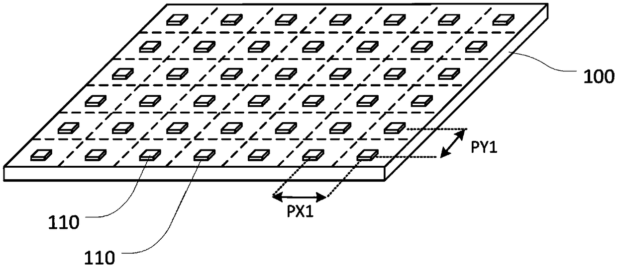
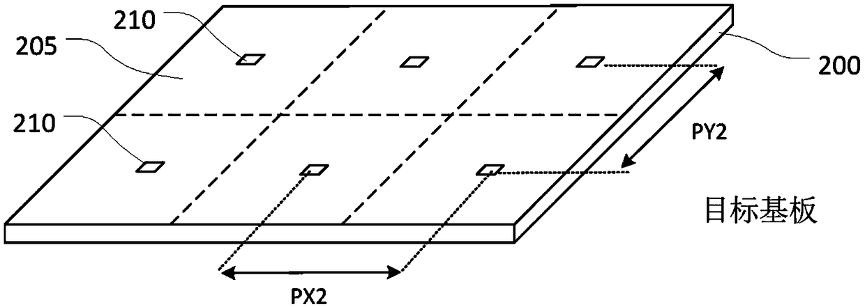
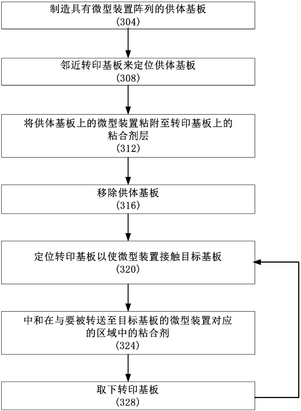
[0045] In order to fabricate some devices, new technologies are needed to accurately and economically provide microdevices on substrates such as large-area substrates or flexible substrates. For example, it is desirable to provide LED panels based on III-V semiconductor technology because micro-LEDs have significant brightness, lifetime and efficiency advantages over organic light emitting diode (OLED) devices.

[0046] A method for fabricating a device comprising an array of individual microdevices is to fabricate the microdevices together on an initial substrate and then transfer the microdevices to a receiving or target substrate that will form part of the product. One reason for building microdevices on an initial substrate is that the target substrate may be a material that is incompatible with the fabrication processes such as etching and deposition required to form the microdevices. In the case of LEDs, for example, deposition of LEDs is an epitaxial growth process in w...


PUM


Abstract

A method of surface mounting micro-devices includes adhering a first plurality of micro-devices on a donor substrate to a transfer surface with an adhesive layer, removing the first plurality of micro-devices from donor substrate while the first plurality of micro-devices remain adhered to the transfer surface, positioning the transfer surface relative to a destination substrate so that a subset of the plurality of micro-devices on the transfer surface abut a plurality of receiving positions on the destination substrate, the subset including one or more micro-devices but less than all of micro-devices of the plurality of micro-devices, selectively neutralizing one or more of regions of the adhesive layer on the transfer surface corresponding to the subset of micro-device to light to detachthe subset of micro-devices from the adhesive layer, and separating the transfer surface from the destination substrate such that the subset of micro-devices remain on the destination substrate.

Description

technical field [0001] The present disclosure generally relates to the transfer of microdevices from a donor substrate to a target substrate. Background technique [0002] Many products contain arrays of individual devices on a substrate, where the devices are addressable or controlled by circuitry on the substrate. A device can be considered a micro-device when the individual devices are on the micron scale (eg, less than 100 microns across). In general, microdevices can be fabricated using a series of microfabrication techniques such as deposition, photolithography and etching to deposit and pattern a series of layers. [0003] One method for fabricating a device comprising an array of individual microdevices is to fabricate the individual microdevices directly on a substrate that will form part of the product. Such techniques have been used, for example, to manufacture TFT panels and color filter panels for active matrix liquid crystal displays (LCDs). [0004] One pro...

Claims


Application Information

Patent Timeline
IPC IPC(8): G03F7/20H01L21/683
CPCH01L25/0753H01L27/156H01L21/6836H01L21/67132H01L33/48H01L33/0093H01L21/67144H01L33/60H01L33/20G03F7/70383G03F7/70825H05K13/0015H05K13/0069H05K13/0469H05K3/0026H05K3/305H01L2221/68322H01L2221/68368H01L2933/0033H01L2221/68381H01L33/0095H01L21/6835
Inventor 曼尼凡南·托塔德里罗伯特·詹·维瑟
Owner APPLIED MATERIALS INC
Why Eureka
Try Eureka