Gate double-clamped IGBT devices

A clamping and gate technology, applied in semiconductor devices, electrical components, circuits, etc., can solve the problems of irreversible damage to IGBT gate, increase of collector short-circuit current, device burnout, etc., to improve integration and protect gate electrode , the effect of increasing robustness

Pending Publication Date: 2019-01-11
JIANGSU CAS JUNSHINE TECH
View PDF0 Cites 3 Cited by
  • Summary
  • Abstract
  • Description
  • Claims
  • Application Information

AI Technical Summary

Problems solved by technology

In the actual application circuit, the gate of the IGBT will generate positive and negative peaks of the gate voltage when the circuit is working. On the one hand, the existence of the peak may cause irreversible damage to the gate of the IGBT. The sharp increase of the collector short-circuit current eventually causes the device to be burned

Method used


Image

  • Gate double-clamped IGBT devices
  • Gate double-clamped IGBT devices
  • Gate double-clamped IGBT devices

Examples


Embodiment Construction

[0021] The present invention will be further described below in conjunction with specific drawings and embodiments.

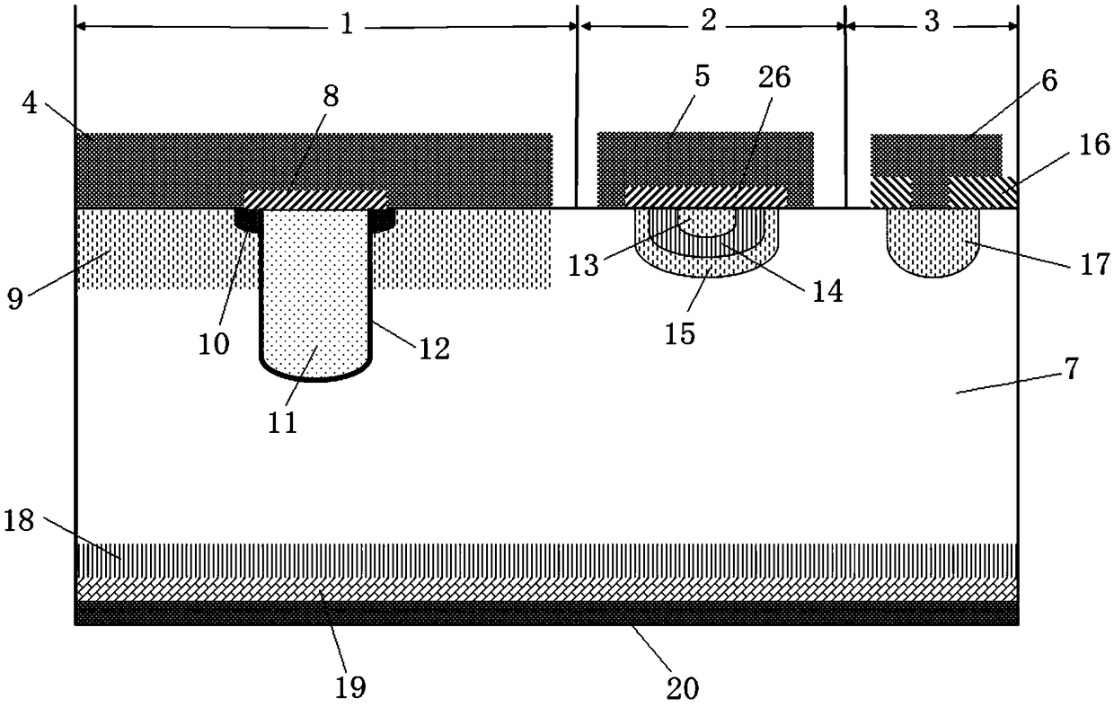
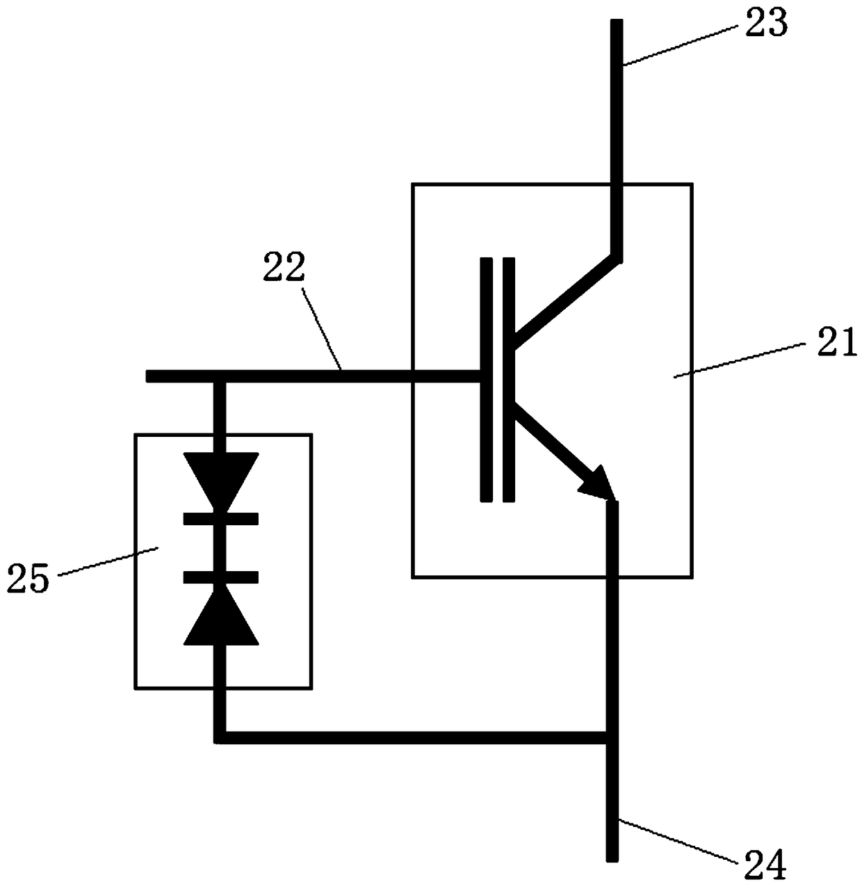
[0022] Such as figure 1 , figure 2 with image 3 Shown: In order to reduce the influence of the gate electrode 22 of the IGBT device 21 by the excessively high positive and negative gate voltage spikes, and to avoid the rapid increase of the short-circuit current when the gate voltage is too high, the IGBT device 21 is burnt, and the N-type IGBT device 21 As an example, the present invention includes a semiconductor substrate and a cell region located in the center of the semiconductor substrate; the cell region includes an emitter region 1 and a gate electrode region 2; the semiconductor substrate includes an N-type drift region 7, and the emitter region 1 includes the emitter metal layer 4, and the gate electrode region 2 includes the gate metal layer 5;

[0023] It also includes a gate voltage clamping structure 25 disposed in the gate electrode region 2. The g...


PUM


Abstract

The invention relates to a gate double-clamped IGBT device. The gate voltage clamping structure includes a third doped region located directly below the gate metal layer, a second doped region locatedin the third doped region, and a first doped region located in the second doped region. The first doping region is located in the first conductivity type drift region, the doping type of the first doping region is consistent with the doping type of the third doping region, and the doping type of the first doping region is different from the doping type of the second doping region. The first dopedregion is in ohmic contact with the gate metal layer, and the third doped region is in ohmic contact with the emitter metal. The invention has a compact structure, reduces the influence of the gate electrode of the IGBT device by the high peak of the positive and negative gate voltage, avoids the short-circuit current sharply increasing when the gate voltage is too high, and leads to the burnoutof the IGBT device, and is safe and reliable.

Description

Technical field [0001] The invention relates to an IGBT device, in particular to an IGBT device with a double-clamped gate, and belongs to the technical field of IGBT devices. Background technique [0002] Insulated gate bipolar transistor (IGBT) is a power electronic device that combines MOS field effect and bipolar transistor; it not only has the advantages of MOSFET easy to drive, simple control, high switching frequency, but also has the conduction voltage of power transistor The advantages of lowering the ground, hitting the same current, and low loss. In view of these advantages of IGBT, it has become the main switching device of today's advanced power electronic devices, which is widely used in various fields of the national economy such as communications, energy, transportation, industry, medicine, household appliances and aerospace. Application of IGBT Played a vital role in the improvement of system performance. [0003] After the development of IGBT in recent years, it...

Claims


Application Information

Patent Timeline
IPC IPC(8): H01L29/739H01L29/06
CPCH01L29/0684H01L29/7395
Inventor 孔凡标许生根张金平姜梅
Owner JIANGSU CAS JUNSHINE TECH
Why Eureka
Try Eureka