Surface-enhanced Raman substrate and preparation method thereof
A surface-enhanced Raman and substrate technology, applied in Raman scattering, ion implantation plating, coating, etc., can solve the problems of limiting the application of SERS substrate detection, affecting the SERS enhancement ability, and weak local electromagnetic field enhancement effect. Strong local electromagnetic field enhancement effect, ultra-high signal enhancement ability, and sensitivity enhancement effect
- Summary
- Abstract
- Description
- Claims
- Application Information
AI Technical Summary
Problems solved by technology
Method used
Image
Examples
preparation example Construction
[0024] Another object of the present invention is to provide a method for preparing the above-mentioned surface-enhanced Raman substrate, which specifically includes the following steps:
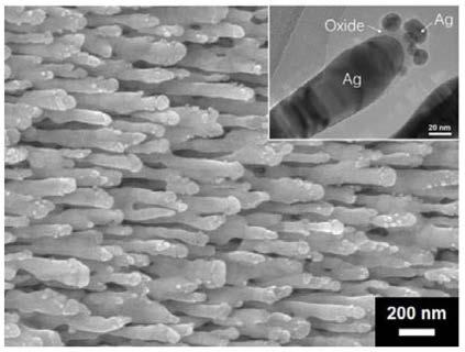
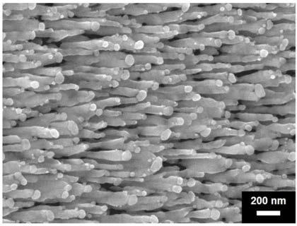
[0025] Using the oblique growth method of electron beam deposition, an ultra-thin oxide layer is deposited on the top of the silver nanorod array; then silver nanoparticles are deposited on the top of the oxide layer to obtain a silver nanorod-oxide-silver particle composite structure as Surface-enhanced Raman substrates.
[0026] The method of preparing an ultra-thin oxide layer by using the oblique growth method is as follows: using a high-melting point oxide as a target material, adjusting the incident angle of the electron beam to 80-88°, and keeping the sample stage stationary, depositing a thickness of 5~20 nm oxide layer.
[0027] The method of preparing silver nanoparticles by using the inclined growth method is as follows: convert the evaporation material to metallic silver, adjust...
Embodiment 1
[0032] 1. Clean the glass substrate sequentially with acetone, alcohol and deionized water and dry it;
[0033] 2. Fix the cleaned substrate on the sample stage of the electron beam evaporation coating machine, and pump the chamber of the electron beam evaporation coating machine to 10 -5 High vacuum below Pa;
[0034] 3. Deposit a 600nm-long silver nanorod array film on the substrate;
[0035] 4. Convert the evaporation material to aluminum oxide, adjust the incident angle of the electron beam to 82°, and make the sample stage static, and deposit an aluminum oxide layer with a thickness of 8 nm on the top of the silver nanorod array;
[0036] 5. Convert the evaporation material to silver metal, the incident angle of the electron beam is 82°, and make the sample stage static, and deposit silver nanoparticles with a thickness of 50 nm on the top of the aluminum oxide layer;
[0037] 6. Heat the silver nanorod-alumina-silver particle substrate prepared in steps 1-5 and the sil...
Embodiment 2
[0040] 1. Clean the glass substrate sequentially with acetone, alcohol and deionized water and dry it;
[0041] 2. Fix the cleaned substrate on the sample stage of the electron beam evaporation coating machine, and pump the chamber of the electron beam evaporation coating machine to 10 -5 High vacuum below Pa;
[0042] 3. Deposit 800 nm-long silver nanorod array film on the substrate of the sample stage;
[0043] 4. Convert the evaporation material to aluminum oxide, adjust the incident angle of the electron beam to 85°, and make the sample stage static, and deposit an aluminum oxide layer with a thickness of 12 nm on the top of the silver nanorod array;
[0044] 5. Convert the evaporation material to metallic silver, the incident angle of the electron beam is 85°, and make the sample stage static, and deposit silver nanoparticles with a thickness of 150 nm on the top of the aluminum oxide layer;
[0045] 6. Configure 10 -6 mol / L methylene blue solution;
[0046] 7. Put the...
PUM
 Abstract
Description
Claims
Application Information
 - R&D
- Intellectual Property
- Life Sciences
- Materials
- Tech Scout
- Unparalleled Data Quality
- Higher Quality Content
- 60% Fewer Hallucinations
Browse by: Latest US Patents, China's latest patents, Technical Efficacy Thesaurus, Application Domain, Technology Topic, Popular Technical Reports.
© 2025 PatSnap. All rights reserved.Legal|Privacy policy|Modern Slavery Act Transparency Statement|Sitemap|About US| Contact US: help@patsnap.com


