A method for manufacturing a high-frequency silicon capacitor

A technology of silicon capacitors and manufacturing methods, which is applied to electric solid devices, circuits, electrical components, etc., can solve the problems of low operating frequency of silicon capacitors, the inability to use advanced 3D packaging in capacitor packaging forms, and low operating frequency, and achieves the improvement of silicon capacitors. Intra-chip uniformity, good step coverage, and improved capacity accuracy

Inactive Publication Date: 2018-12-14
无锡中微晶园电子有限公司
View PDF3 Cites 0 Cited by
  • Summary
  • Abstract
  • Description
  • Claims
  • Application Information

AI Technical Summary

Problems solved by technology

[0002] With the miniaturization of electronic products and the increase in communication speed, traditional capacitors cannot be packaged in advanced 3D packaging. More importantly, the operating frequency is limited, generally working below 10G, which cannot meet the needs of the 5G communication era. needs
[0003] Silicon capacitors are a new member of the capacitor family. The existing silicon capacitors use LPCVD to deposit ONO (silicon dioxide / silicon nitride / silicon dioxide) as their dielectric. It has mature technology and low dielectric constant. ONO dielectric Manufactured silicon capacitors have a low operating frequency, generally only up to a few megahertz. Due to its low operating frequency, its reliability is poor
The working frequency of the capacitor is determined by the polarization time of the capacitor medium. The ONO medium of a conventional silicon capacitor is a laminated structure, which is an amorphous ionic crystal with a relaxed structure. The relaxation polarization of electrons and ions takes a certain amount of time, so resulting in lower frequency

Method used


Image

  • A method for manufacturing a high-frequency silicon capacitor
  • A method for manufacturing a high-frequency silicon capacitor
  • A method for manufacturing a high-frequency silicon capacitor

Examples


Embodiment Construction

[0036] The present invention will be further described below in conjunction with specific drawings and embodiments.

[0037] The embodiment of the present invention takes an N-type high-frequency silicon capacitor as an example, the first conductivity type is N-type, and the second conductivity type is P-type. A method for manufacturing a high-frequency silicon capacitor is characterized in that it includes the following step:

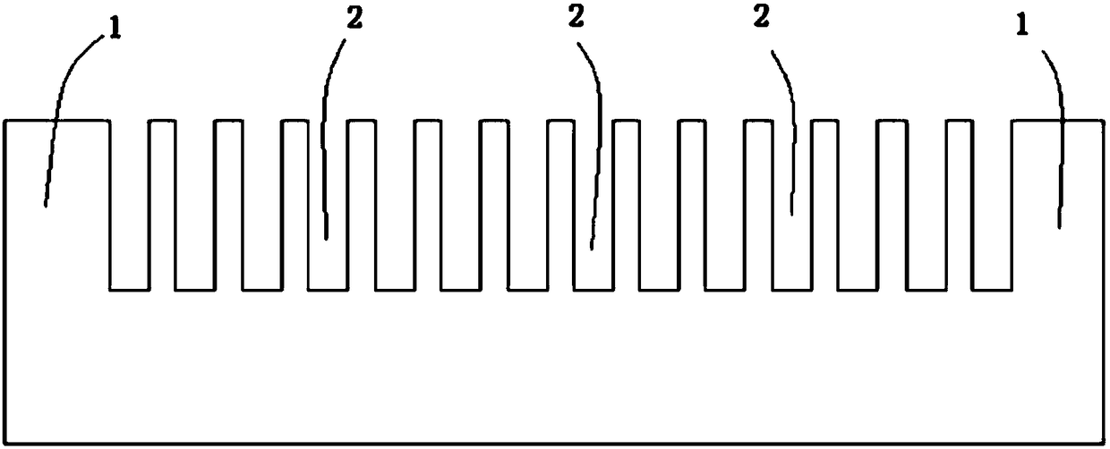
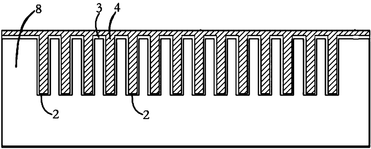
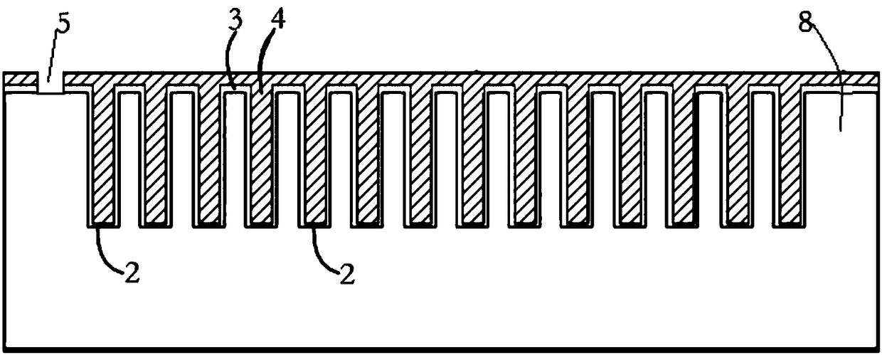
[0038] Such as figure 1 As shown, step 1. Provide a P-type substrate 1, etch several grooves 2 on the P-type substrate 1;

[0039] Specifically, before etching the trench 2, a layer of SiO is grown on the surface of the P-type substrate 1. 2 Masking layer 10, SiO 2 The thickness of masking layer 10 is about 1200nm, etching SiO 2 masking layer 10, resulting in SiO 2 masking window, the SiO 2 Under the cover of the masking window, etch the P-type substrate 1 to obtain several trenches 2 in the P-type substrate 1, the width of the trenches 2 is 1-3...


PUM

PropertyMeasurementUnit
Thicknessaaaaaaaaaa
Thicknessaaaaaaaaaa

Abstract

The invention belongs to the technical field of semiconductor manufacturing and relates to a method for manufacturing a high-frequency silicon capacitor. The method includes etching a plurality of trenches on a substrate, forming an HfO2 dielectric layer by atomic deposition technology, depositing polycrystalline silicon on the surface of the HfO2 dielectric layer, etching to form vias, depositingan insulating layer, etching to form metal contact vias, and sputtering metal to form electrodes. The method of the invention adopts the latest atomic deposition technology to manufacture the HfO2 dielectric layer, so that the frequency characteristic of the silicon capacitor is superior to that of the traditional capacitor, the reliability is high, the capacitance precision of the capacitor is greatly improved, and the finished product rate is improved.

Description

technical field [0001] The invention relates to a method for a silicon capacitor, in particular to a method for manufacturing a high-frequency silicon capacitor, and belongs to the technical field of semiconductor manufacturing. Background technique [0002] With the miniaturization of electronic products and the increase in communication speed, traditional capacitors cannot be packaged in advanced 3D packaging. More importantly, the operating frequency is limited, generally working below 10G, which cannot meet the needs of the 5G communication era. demand. [0003] Silicon capacitors are a new member of the capacitor family. The existing silicon capacitors use LPCVD to deposit ONO (silicon dioxide / silicon nitride / silicon dioxide) as their dielectric. It has mature technology and low dielectric constant. ONO dielectric The manufactured silicon capacitors have a low operating frequency, generally only up to a few megahertz, and because of its low operating frequency, its rel...

Claims


Application Information

Patent Timeline
IPC IPC(8): H01L23/64
Inventor 肖志强陈杰高向东王涛
Owner 无锡中微晶园电子有限公司
Why Eureka
Try Eureka