


Quick Research
Generate reliable direction feasibility study reports for your R&D in just a few steps.

Technical Q&A
Discover and master advanced knowledge NOW. Basics, ideas, possibilities, all at once.

Find Solutions
As an expert in R&D theories, this can generate solutions to your technical problems instantly.

Evaluate Feasibility
Analyze your overall solution with one click, know your potential R&D risks in advance.

Monitor Landscape
Get weekly tech updates, stay abreast of the latest tech innovations and key insights.
A kind of insulated gate bipolar transistor with quantum dot structure
A technology of bipolar transistors and quantum dots, applied in semiconductor devices, semiconductor/solid-state device manufacturing, electrical components, etc. Effect of tail current and buffer thickness
- Summary
- Abstract
- Description
- Claims
- Application Information
AI Technical Summary
Problems solved by technology
Method used
Image

Examples
Embodiment 1
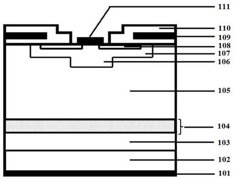
[0026] An insulated gate bipolar transistor (IGBT) with a quantum dot structure, comprising: a drain 101, a P + GaN substrate 102, N-type GaN buffer layer 103, N-type InGaN / GaN quantum dot layer 104, N-type - GaN base region 105, P + Well 106, P base region 107, N + Contact region 108 , gate 109 , gate dielectric layer 110 and source 111 .
[0027] in:
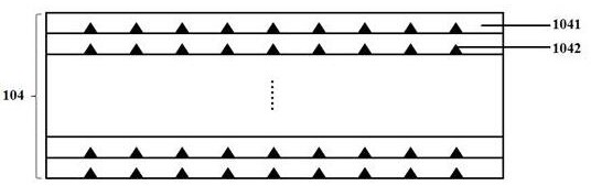
[0028] The structure of the N-type quantum dot layer 104 is as follows image 3 As shown, a GaN layer 1041 and InGaN 1042 quantum dots are included.
[0029] The InGaN quantum dots are uniformly distributed, with a size of 5 nm and a density of 5×10 9 cm -2 .
[0030] The N-type buffer layer 103 has a thickness of 5 μm, and the N-type InGaN / GaN quantum dot layer 104 has a thickness of 100 nm, N - The thickness of the base region 105 is 30 μm.
[0031] The substrate 102 is P + GaN substrate.
[0032] The N - The base region 105 and the N-type quantum dot layer 104 are doped with Si, and the electron concentration ...
Embodiment 2
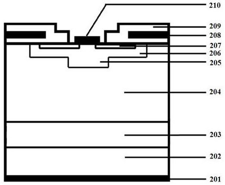
[0037] An insulated gate bipolar transistor (IGBT) with a quantum dot structure, comprising: a drain 101, a P + Si substrate 102, N-type Si buffer layer 103, N-type Ge / Si quantum dot layer 104, N - Si base region 105, P + Well 106, P base region 107, N + Contact region 108 , gate 109 , gate dielectric layer 110 and source 111 .
[0038] in:
[0039] The structure of the N-type quantum dot layer 104 is as follows Figure 4 As shown, a Si layer 1043 and Ge1044 quantum dots are included.
[0040] The Ge quantum dots are randomly distributed, with a size of 5 nm and a density of 5×10 9 cm-2 .
[0041] The thickness of the N-type buffer layer 103 is 5 μm, the thickness of the N-type Ge / Si quantum dot layer 104 is 100 nm, and the thickness of N - The thickness of the base region 105 is 30 μm.
[0042] The substrate 102 is P + Si substrate.
[0043] The N - The base region 105 and the N-type quantum dot layer 104 are doped with P, and the electron concentration therein i...
PUM
 Abstract
Description
Claims
Application Information
 - R&D Engineer
- R&D Manager
- IP Professional
- Industry Leading Data Capabilities
- Powerful AI technology
- Patent DNA Extraction
Browse by: Latest US Patents, China's latest patents, Technical Efficacy Thesaurus, Application Domain, Technology Topic, Popular Technical Reports.
© 2024 PatSnap. All rights reserved.Legal|Privacy policy|Modern Slavery Act Transparency Statement|Sitemap|About US| Contact US: help@patsnap.com