Klystron TESLA theory input cavity coupling term processing method
A klystron and input chamber technology, applied in klystrons, electron tubes with velocity/density modulation electron flow, electrical digital data processing, etc., can solve problems that have not been clearly raised
- Summary
- Abstract
- Description
- Claims
- Application Information
AI Technical Summary
Problems solved by technology
Method used
Image
Examples
Embodiment Construction
[0066] Embodiments of the present invention will be further described in detail below in conjunction with the accompanying drawings and examples.
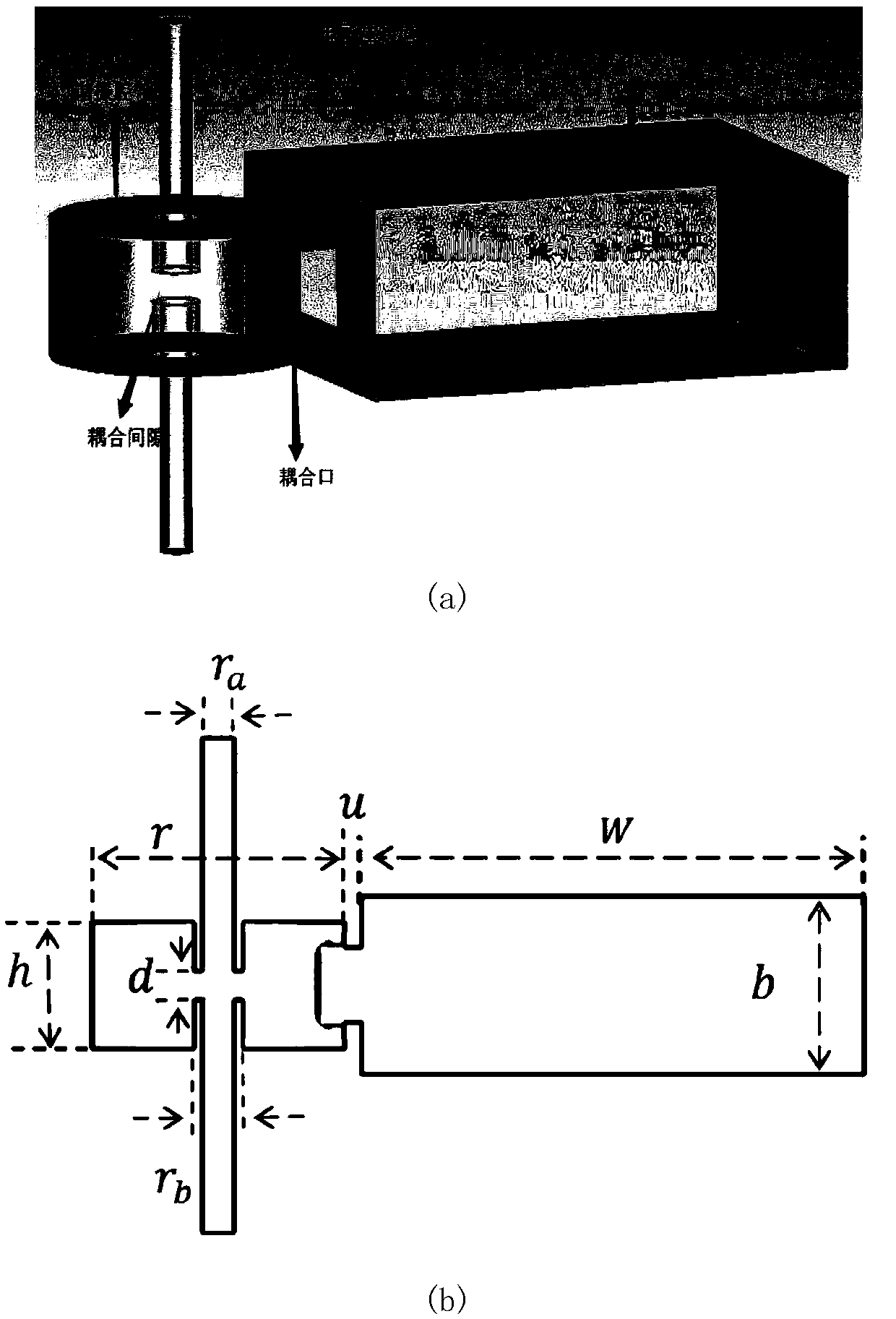
[0067] The example adopts the S-band klystron input cavity to carry out the calculation of the electromagnetic field. Various size parameters such as figure 2 As shown in (b), the detailed size parameters are shown in Table 1.
[0068] Table 1 Klystron size parameters (unit: mm)
[0069] r a
r b
r
h
d
u
w
b
4.00
6.00
31.20
15.50
7.00
4.00
124.00
43.48
[0070] r in table 1 a Represents the diameter of the electron beam channel, r and h represent the diameter and height of the double-entry resonator respectively, d represents the length of the coupling gap, u represents the length of the coupling hole, and the coupling hole corresponds to the broadside k of the waveguide a =36.27mm, narrow side k b =18.26mm, wide side a of the input waveguide=86.36mm, narrow side b...
PUM
 Abstract
Description
Claims
Application Information
 - R&D Engineer
- R&D Manager
- IP Professional
- Industry Leading Data Capabilities
- Powerful AI technology
- Patent DNA Extraction
Browse by: Latest US Patents, China's latest patents, Technical Efficacy Thesaurus, Application Domain, Technology Topic, Popular Technical Reports.
© 2024 PatSnap. All rights reserved.Legal|Privacy policy|Modern Slavery Act Transparency Statement|Sitemap|About US| Contact US: help@patsnap.com


