


Quick Research
Generate reliable direction feasibility study reports for your R&D in just a few steps.

Technical Q&A
Discover and master advanced knowledge NOW. Basics, ideas, possibilities, all at once.

Find Solutions
As an expert in R&D theories, this can generate solutions to your technical problems instantly.

Evaluate Feasibility
Analyze your overall solution with one click, know your potential R&D risks in advance.

Monitor Landscape
Get weekly tech updates, stay abreast of the latest tech innovations and key insights.
Solar cell and preparation method therefor
A solar cell, N-type technology, applied in the field of solar cells, can solve the problems of reduced photoelectric conversion efficiency of organic-inorganic hybrid solar cells, poor film formation quality of organic material layers, low photoelectric conversion efficiency of solar cells, etc. Conversion efficiency, improved quality, improved transmission path effect
- Summary
- Abstract
- Description
- Claims
- Application Information
AI Technical Summary
Problems solved by technology
Method used
Image

Examples
preparation example Construction
[0026] A kind of preparation method of solar cell that the present invention proposes, comprises the following steps:
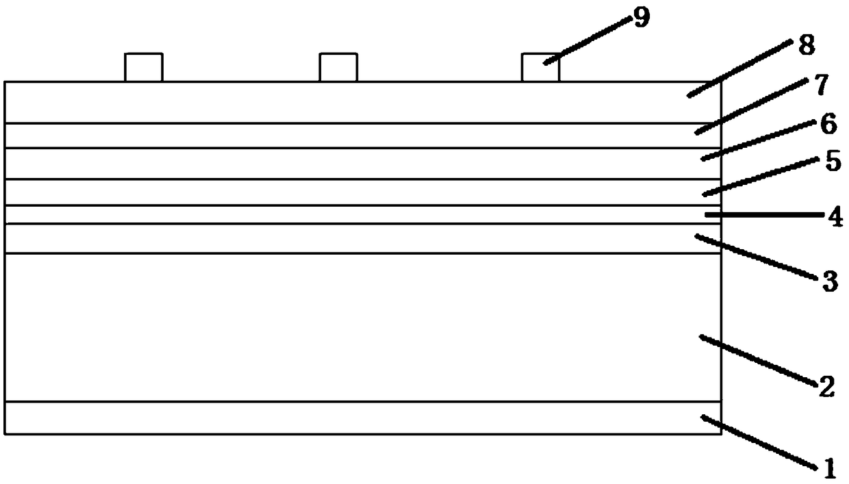
[0027] 1) Provide N-type monocrystalline silicon wafers, carry out texturing treatment to the N-type monocrystalline silicon wafers, and form a pyramid-structured textured layer on the upper surface of the N-type monocrystalline silicon wafers;
[0028] 2) Depositing an N-type amorphous silicon layer on the upper surface of the N-type single crystal silicon wafer, and then converting the N-type amorphous silicon layer into an N-type polysilicon layer through heat treatment, wherein the doping concentration of the N-type polysilicon layer is less than The doping concentration of the N-type monocrystalline silicon wafer, specifically, the heat treatment temperature is 600-800°C, the heat treatment time is 20-40 minutes, and the thickness of the N-type polysilicon layer is 20-30 nanometers;
[0029] 3) depositing an inorganic insulating thin layer on the surface...
Embodiment 1
[0039] A method for preparing a solar cell, comprising the steps of:
[0040] 1) Provide N-type monocrystalline silicon wafers, carry out texturing treatment to the N-type monocrystalline silicon wafers, and form a pyramid-structured textured layer on the upper surface of the N-type monocrystalline silicon wafers;
[0041] 2) Depositing an N-type amorphous silicon layer on the upper surface of the N-type monocrystalline silicon wafer, and then converting the N-type amorphous silicon layer into an N-type polysilicon layer through heat treatment, wherein the doping concentration of the N-type polysilicon layer is less than The doping concentration of the N-type monocrystalline silicon wafer, specifically, the heat treatment temperature is 700°C, the heat treatment time is 30 minutes, and the thickness of the N-type polysilicon layer is 25 nanometers;
[0042] 3) depositing an inorganic insulating thin layer on the surface of the N-type polysilicon layer, the thickness of the ino...
Embodiment 2
[0052] A method for preparing a solar cell, comprising the steps of:
[0053] 1) Provide N-type monocrystalline silicon wafers, carry out texturing treatment to the N-type monocrystalline silicon wafers, and form a pyramid-structured textured layer on the upper surface of the N-type monocrystalline silicon wafers;
[0054] 2) Depositing an N-type amorphous silicon layer on the upper surface of the N-type monocrystalline silicon wafer, and then converting the N-type amorphous silicon layer into an N-type polysilicon layer through heat treatment, wherein the doping concentration of the N-type polysilicon layer is less than The doping concentration of the N-type monocrystalline silicon wafer, specifically, the heat treatment temperature is 600°C, the heat treatment time is 40 minutes, and the thickness of the N-type polysilicon layer is 30 nanometers;
[0055] 3) depositing an inorganic insulating thin layer on the surface of the N-type polysilicon layer, the thickness of the ino...
PUM
| Property | Measurement | Unit |
|---|---|---|
| thickness | aaaaa | aaaaa |
| thickness | aaaaa | aaaaa |
| thickness | aaaaa | aaaaa |
Abstract
Description
Claims
Application Information
 - R&D Engineer
- R&D Manager
- IP Professional
- Industry Leading Data Capabilities
- Powerful AI technology
- Patent DNA Extraction
Browse by: Latest US Patents, China's latest patents, Technical Efficacy Thesaurus, Application Domain, Technology Topic, Popular Technical Reports.
© 2024 PatSnap. All rights reserved.Legal|Privacy policy|Modern Slavery Act Transparency Statement|Sitemap|About US| Contact US: help@patsnap.com