Image sensor and formation method thereof

A technology of image sensors and optoelectronic devices, applied in the direction of electric solid-state devices, semiconductor devices, electrical components, etc., can solve the problems of quantum conversion efficiency that needs to be improved, and achieve the effects of improving quantum conversion efficiency, improving light crosstalk, and improving performance

Active Publication Date: 2018-11-23
淮安西德工业设计有限公司
View PDF4 Cites 2 Cited by
  • Summary
  • Abstract
  • Description
  • Claims
  • Application Information

AI Technical Summary

Problems solved by technology

[0004] Quantum conversion efficiency (QE, Quantum Efficiency) is one of the important indicators affecting the performance of image sensors, and the quantum conversion efficiency of existing back-illuminated image sensors still needs to be improved

Method used


Image

  • Image sensor and formation method thereof
  • Image sensor and formation method thereof
  • Image sensor and formation method thereof

Examples


Embodiment Construction

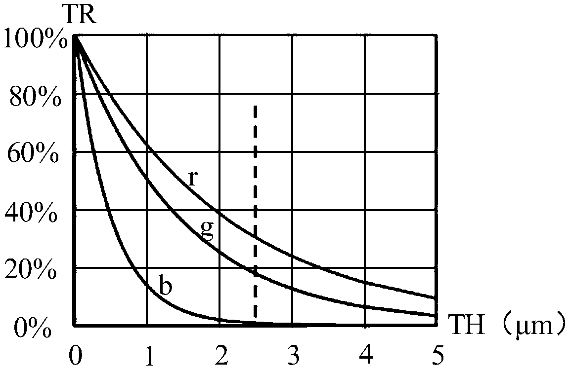
[0026] Such as figure 1 As shown, taking an RGB image sensor as an example, the transmittance (TR, transmittance) of different wavelengths of light on semiconductor substrates with different thicknesses gradually decreases as the thickness (TH, thickness) of the semiconductor substrate increases. In comparison, the light transmittance of red light r is higher than that of green light g, and the light transmittance of green light g is higher than that of blue light b. At present, the R / G / B pixels of the back-illuminated image sensor are produced in the silicon substrate with the same thickness (such as 2.5 μm ~ 3.0 μm), and the blue light b (light transmittance is about 0%) is almost completely absorbed, while some Red light r (light transmittance is about 20% to 30%) and green light g (light transmittance is about 10% to 20%) penetrate the silicon substrate, which reduces the quantum conversion efficiency of light and also produces Light crosstalk and other issues.

[0027] ...


PUM


Abstract

The technical scheme of the invention discloses an image sensor and a formation method thereof. The image sensor comprises a semiconductor substrate, a shallow groove isolation structure, a device structure and a reflecting layer, wherein the semiconductor substrate is divided into a plurality of regions, a photoelectric device is formed in the semiconductor substrate at each region, each region of the semiconductor substrate is provided with a protruding surface, the width of the protruding surface is adaptive to the size of the photoelectric device, the shallow groove isolation structure isformed in the semiconductor substrate and is arranged among the photoelectric devices, the device structure is arranged on the semiconductor substrate and in the semiconductor substrate, the reflecting layer is formed on the semiconductor substrate with the protruding surfaces, and the shallow groove isolation structure and the device structure are exposed. With the image sensor disclosed by the technical scheme, the quantum conversion efficiency of the image sensor is improved.

Description

technical field [0001] The invention relates to the field of manufacturing semiconductor devices, in particular to an image sensor and a forming method thereof. Background technique [0002] An image sensor is a semiconductor device that converts light signals into electrical signals. Image sensors are classified into complementary metal oxide (CMOS) image sensors and charge coupled device (CCD) image sensors. CMOS image sensor has the advantages of simple process, easy integration of other devices, small size, light weight, low power consumption and low cost. Therefore, with the development of image sensing technology, CMOS image sensors are increasingly used in various electronic products instead of CCD image sensors. At present, CMOS image sensors have been widely used in still digital cameras, digital video cameras, medical imaging devices, and automotive imaging devices. [0003] CMOS image sensors include front illuminated (FSI) image sensors and back illuminated (B...

Claims


Application Information

Patent Timeline
Patent Type & Authority Applications(China)
IPC IPC(8): H01L27/146
CPCH01L27/146H01L27/14601H01L27/14629H01L27/14683
Inventor 何延强林宗德黄仁德
Owner 淮安西德工业设计有限公司
Why Eureka
Try Eureka