
Epitaxial structure of a light emitting diode and its manufacturing method

A technology of light-emitting diodes and epitaxial structures, which is applied in the direction of semiconductor devices, electrical components, circuits, etc., can solve the problems of affecting the service life of light-emitting diodes, unfavorable recombination of electrons and holes, and reducing the luminous efficiency of light-emitting diodes. Luminescence, improving the effect of lattice constant mutations, reducing the effect of density

Active Publication Date: 2019-10-29
HC SEMITEK ZHEJIANG CO LTD
View PDF7 Cites 0 Cited by
  • Summary
  • Abstract
  • Description
  • Claims
  • Application Information

AI Technical Summary

Problems solved by technology

[0006] Although the aluminum nitride buffer layer can alleviate the lattice mismatch between the sapphire substrate (the main material is aluminum oxide) and the gallium nitride material, the lattice constant of sapphire is 4.758, and the lattice constant of aluminum nitride is 3.110. There is still a large lattice mismatch between the sapphire substrate and the aluminum nitride buffer layer, resulting in poor crystal quality of the aluminum nitride buffer layer formed on the sapphire substrate, and the intersection of the sapphire substrate and the aluminum nitride buffer layer There is a large stress at the interface, which affects the crystal quality of the subsequent active layer, etc., and the active layer has problems such as leakage and dislocation line generation, which is not conducive to the recombination of electrons and holes and reduces the luminous efficiency of the light-emitting diode. It will produce large-density defects, accelerate the aging of light-emitting diodes, and affect the service life of light-emitting diodes

Method used


Image

  • Epitaxial structure of a light emitting diode and its manufacturing method
  • Epitaxial structure of a light emitting diode and its manufacturing method
  • Epitaxial structure of a light emitting diode and its manufacturing method

Examples


Embodiment Construction

[0028] In order to make the object, technical solution and advantages of the present invention clearer, the implementation manner of the present invention will be further described in detail below in conjunction with the accompanying drawings.

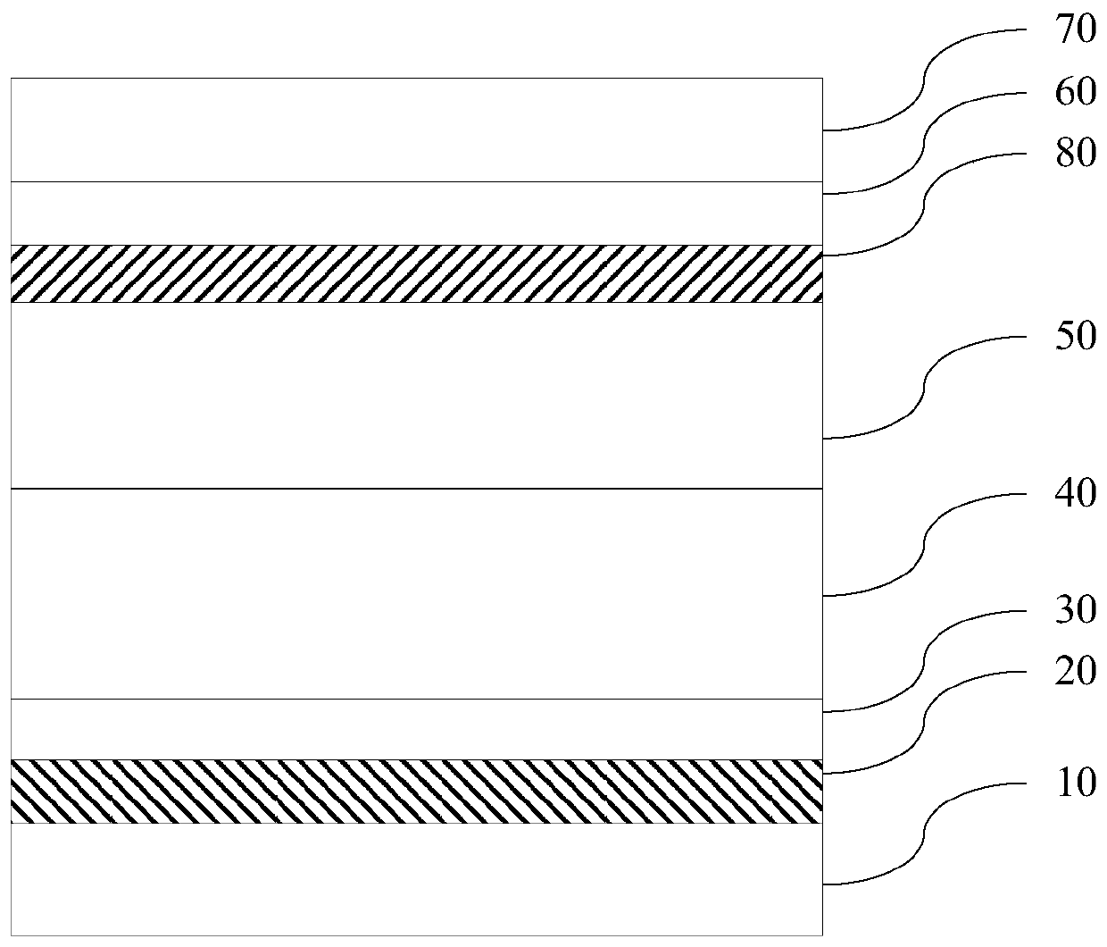
[0029] An embodiment of the present invention provides an epitaxial structure of a light emitting diode, figure 1 For the structural schematic diagram of the epitaxial structure provided by the embodiment of the present invention, see figure 1 , the epitaxial structure includes a sapphire substrate 10, a composite structure 20, a gallium nitride buffer layer 30, an undoped gallium nitride layer 40, an N-type semiconductor layer 50, an active layer 60 and a P-type semiconductor layer 70, and the composite structure 20 , GaN buffer layer 30 , undoped GaN layer 40 , N-type semiconductor layer 50 , active layer 60 and P-type semiconductor layer 70 are stacked on the sapphire substrate 10 in sequence.

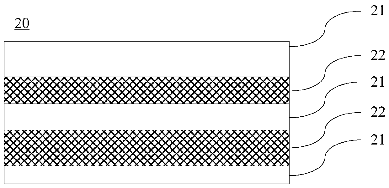
[0030] figure 2 For the structural...


PUM

PropertyMeasurementUnit
thicknessaaaaaaaaaa
thicknessaaaaaaaaaa
thicknessaaaaaaaaaa

Abstract

The invention discloses an epitaxial structure of an LED and a manufacturing method of the epitaxial structure, and belongs to the technical field of semiconductors. The epitaxial structure comprisesa sapphire substrate, and a composite structure, a gallium nitride buffer layer, a non-doped gallium nitride layer, an N type semiconductor layer, an active layer and a P type semiconductor layer laminated on the sapphire substrate respectively; the composite structure comprises (n+1) first sub layers and n second sub layers, n represents a positive integer, and the (n+1) first sub layers and n second sub layers are laminated alternatively; and each first sub layer is an aluminum nitride layer, and each second sub layer is an alumina layer. The aluminum nitride layers and the alumina layers are laminated alternatively on the alumina sapphire whose main component is alumina, the crystal lattice characteristic is changed from transition from alumina to aluminum nitride to dispersion from oneinterface to the whole composite structure, the influence of abrupt change of a crystal lattice constant is changed, a stress generated by crystal lattice mismatch is dispersed effectively and avoided from being too concentrated, and the crystal quality of an active layer and the like formed subsequently can be improved.

Description

technical field [0001] The invention relates to the technical field of semiconductors, in particular to an epitaxial structure of a light emitting diode and a manufacturing method thereof. Background technique [0002] A light-emitting diode (English: Light Emitting Diode, referred to as: LED) is a semiconductor electronic component that can emit light. As a high-efficiency, environmentally friendly and green new-generation solid-state lighting source, LED has the advantages of low voltage, low power consumption, small size, light weight, long life, and high reliability. [0003] Gallium Nitride (GaN) is a semiconductor material with a wide bandgap. The bandgap width is about 3.4eV, which can meet the conditions for the generation of blue light with high photon energy. The blue light can excite the phosphor to emit yellow light, and the yellow light and blue light Mix to create white light. Therefore, since the gallium nitride-based LED was successfully developed by Japane...

Claims


Application Information

Patent Timeline
Patent Type & Authority Patents(China)
IPC IPC(8): H01L33/12H01L33/32H01L33/26
CPCH01L33/12H01L33/26H01L33/32
Inventor 兰叶顾小云
Owner HC SEMITEK ZHEJIANG CO LTD
Learn More