
A kind of ultraviolet light-emitting diode with flip-chip structure

A technology of light-emitting diodes and diodes, applied in semiconductor devices, electrical components, circuits, etc., can solve the problems of low light-emitting efficiency and large turn-on voltage of ultraviolet LEDs, and achieve the effect of alleviating the effect of current congestion

Active Publication Date: 2019-09-10
SOUTHEAST UNIV
View PDF5 Cites 0 Cited by
  • Summary
  • Abstract
  • Description
  • Claims
  • Application Information

AI Technical Summary

Problems solved by technology

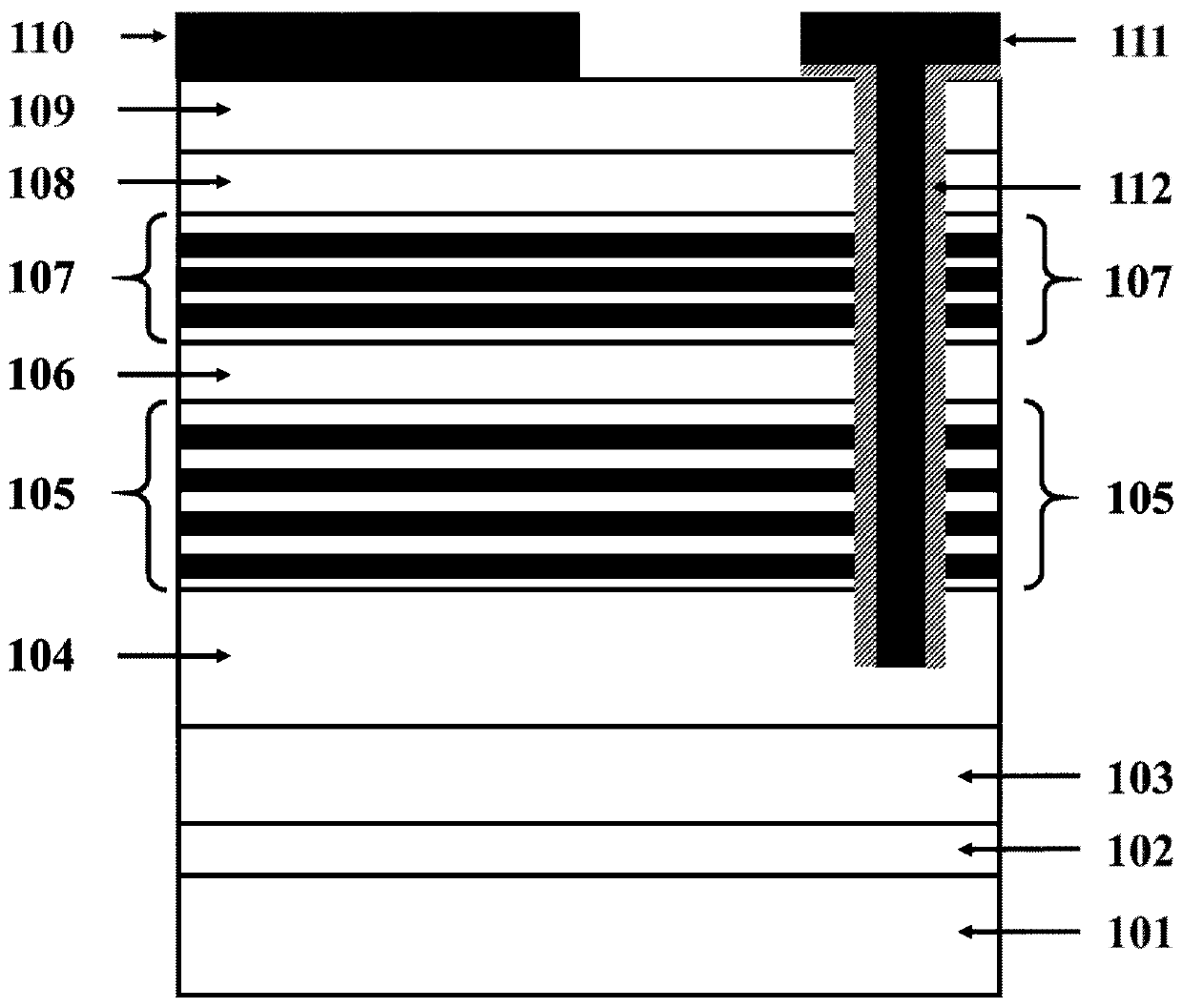
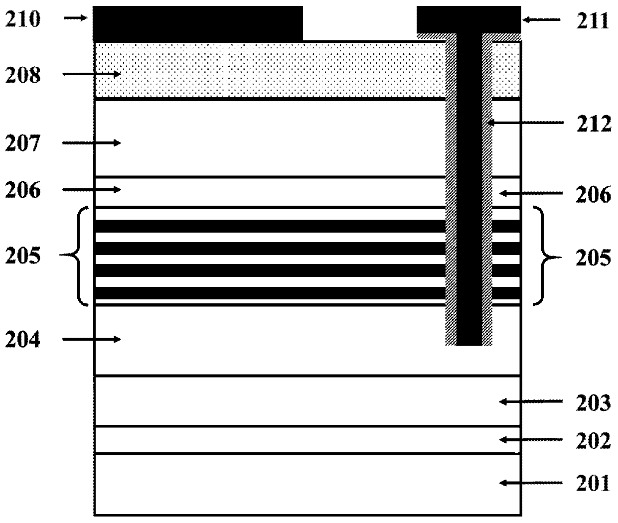
[0006] Technical problem: The object of the present invention is to provide a UV light-emitting diode with a flip-chip structure. On the one hand, the structure uses AlGaN-BN DBR as the p-type region of the UV LED, and on the other hand, BN is used as the EBL of the UV LED. Therefore, it can It fundamentally solves the problems of low light extraction efficiency and high turn-on voltage of the ultraviolet LED with the traditional flip-chip structure; moreover, on the p-type region of the DBR, the flip-chip structure provided by the present invention can still use the currently developed mature heavily doped p- GaN ohmic contact layer and ITO material transparent conductive layer process and technology, so that the current congestion effect that occurs during current injection can be effectively alleviated

Method used


Image

  • A kind of ultraviolet light-emitting diode with flip-chip structure
  • A kind of ultraviolet light-emitting diode with flip-chip structure

Examples


Embodiment 1

[0037] An ultraviolet light-emitting diode structure with a flip-chip structure, the diode includes a substrate 101, an AlN nucleation layer 102, an undoped AlN buffer layer 103, an n-type Al 0.5 Ga 1-0.5 N zone 104, Al 0.45 Ga 0.55 N-Al 0.6 Ga 0.4 N multi-quantum well active region 105, BN electron blocking layer 106, Al 0.6 Ga 0.4 N-BN Bragg mirror structure p-type region 107, heavily doped p-type GaN layer 108 and ITO conductive layer 109, on which a p-type ohmic electrode 110 is arranged in contact with, on the n-type Al 0.5 Ga 0.5 On the N region 104, an n-type ohmic electrode 111 is also arranged in contact, and the n-type ohmic electrode 111 penetrates other regions upwards and extends out of the ITO conductive layer 109, which is different from the n-type Al 0.5 Ga 0.5 An insulating layer 112 is disposed between regions other than the N region 104;

[0038] in:

[0039] The thickness of the BN electron blocking layer 106 is 3nm;

[0040] The Al 0.6 Ga 0.4 ...


PUM


Abstract

The invention provides an ultraviolet light emitting diode with an inverted structure, which comprises a substrate, an AlN nucleation layer, an un-doped AlN or AlaGa1-aN buffer layer, an n-type AlbGa1-bN region, an AlcGa1-cN-AldGa1-dN multi-quantum well active region, a BN electronic barrier layer, an AleGa1-eN-BN Bragg reflector structure p-type region, a heavily-doped p-type GaN layer, an ITO conductive layer, a p-type ohmic electrode arranged on the ITO conductive layer and an n-type ohmic electrode arranged on the n-type AlbGa1-bN layer sequentially from bottom to top. The n-type ohmic electrode and other regions except the n-type AlbGa1-bN layer are insulated. According to the ultraviolet light emitting diode with an inverted structure, the light emitting efficiency of the ultravioletLED can be effectively improved, and the threshold voltage and the resistivity of the ultraviolet LED can be greatly reduced.

Description

technical field [0001] The invention relates to an ultraviolet light-emitting diode (LED) with an inverted structure, belonging to the field of compound semiconductor optoelectronic materials and ultraviolet LED manufacturing. Background technique [0002] Due to its high photon energy and strong penetrating ability, ultraviolet light is widely used in sterilization, water and air purification, solid-state lighting, detection of biochemical harmful substances, high-density storage, and military communications. [0003] AlGaN material is the core material for making UV LEDs. First of all, Al n Ga 1-n N material is a wide band gap direct band gap semiconductor material (0<n<1), by adjusting the ternary compound Al n Ga 1-n Al component n in N, can achieve Al n Ga 1-n The energy of the N bandgap varies continuously between 3.4 and 6.2eV, thereby obtaining ultraviolet light with a wavelength ranging from 210 to 365nm. Second, Al n Ga 1-n N is a compound with stron...

Claims


Application Information

Patent Timeline
Patent Type & Authority Patents(China)
IPC IPC(8): H01L33/06H01L33/10H01L33/14
Inventor 张雄吴自力庄喆崔一平
Owner SOUTHEAST UNIV
Learn More