Wavelength-tunable semiconductor laser
A technology of semiconductors and lasers, which is applied in the direction of semiconductor lasers, lasers, and devices for controlling laser output parameters. It can solve the problems that semiconductor lasers do not have wavelength tunable functions, and achieve selective output, high-speed modulation, and 3dB increase The effect of bandwidth
- Summary
- Abstract
- Description
- Claims
- Application Information
AI Technical Summary
Problems solved by technology
Method used
Image


Examples
Embodiment 1
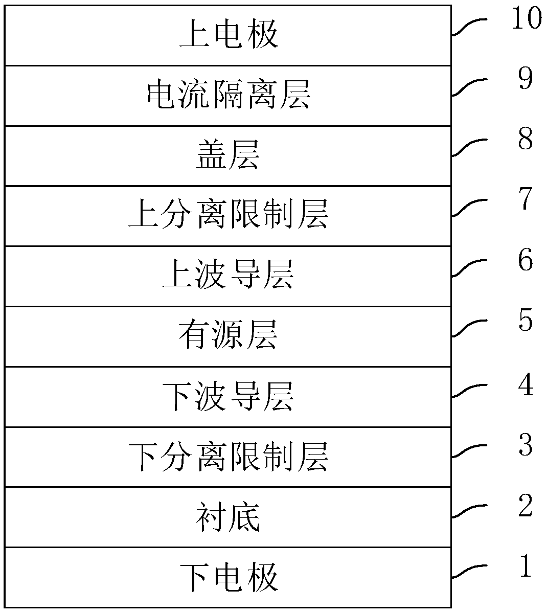
[0046] A wavelength tunable semiconductor laser provided by this embodiment, such as figure 1 As shown, it includes: lower electrode 1, substrate 2, lower separation confinement layer 3, lower waveguide layer 4, active layer 5, upper waveguide layer 6, upper separation confinement layer 7, capping layer 8, current Isolation layer 9, upper electrode 10.
[0047] The lower waveguide layer 4, the active layer 5 and the upper waveguide layer 6 constitute the central region of the optical confinement layer of the semiconductor laser, and the lower separation confinement layer 3 and the upper separation confinement layer 7 constitute the cladding layer of the semiconductor laser.
[0048]The active layer 5 adopts a multilayer quantum well structure in which strained quantum wells and strained quantum barriers are alternately mixed. Preferably, the active layer 5 can be grown with different components of the same material of InGaAsP or AlInGaAs, or grown alternately by two materials...
Embodiment 2
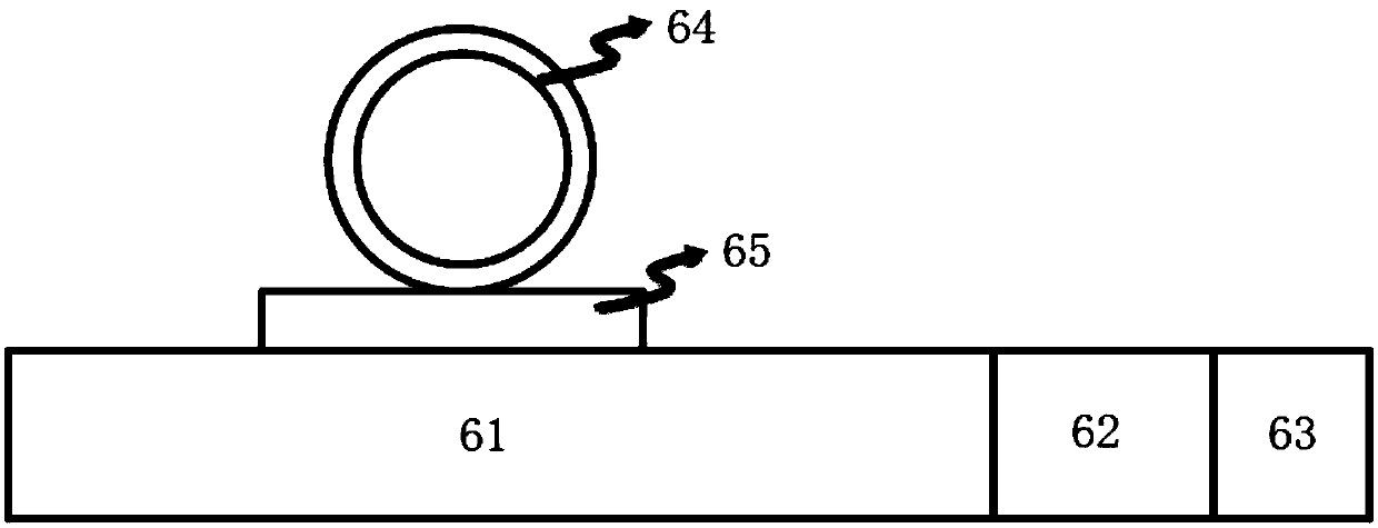
[0061] The difference between this embodiment and Embodiment 1 is that in Embodiment 1, the annular microcavity is directly connected to the ridge waveguide, and there is no electrode on the annular microcavity, but in this embodiment, a side edge is added between the annular microcavity and the ridge waveguide. The electrical isolation area is electrically isolated, and a planar electrode is arranged above the annular microcavity.
[0062] Such as image 3 As shown, a side electrical isolation region 65 is added between the annular microcavity and the ridge waveguide, and a planar electrode is arranged above the annular microcavity, and the electrode of the annular microcavity is connected to the electrode of the gain region 61 and the electrode of the saturable absorption region 63. Independent and not connected, in this way, the wavelength of the semiconductor laser can be adjusted in a small range by adjusting the current injected into the ring microcavity, and the ability...
Embodiment 3
[0064] The difference between this embodiment and Embodiment 1 and Embodiment 2 is that in this embodiment, the microcavity structure adopts a disc-shaped microcavity structure, that is, the upper waveguide layer 6 or the lower waveguide layer 4 adopts a ridge waveguide structure and a disc-shaped The combination of microcavity structure.
[0065] Figure 4 A schematic diagram of the disc-shaped microcavity directly connected to the ridge waveguide without electrodes on the disc-shaped microcavity is given.
[0066] Figure 5 A schematic diagram is shown in which a side electrical isolation region 65 is added between the disk-shaped microcavity and the ridge waveguide for electrical isolation, and a planar electrode is arranged above the disk-shaped microcavity.
[0067] Other structures of this embodiment are the same as those of Embodiment 1 and Embodiment 2, and will not be repeated here.
PUM
 Abstract
Description
Claims
Application Information
 - R&D
- Intellectual Property
- Life Sciences
- Materials
- Tech Scout
- Unparalleled Data Quality
- Higher Quality Content
- 60% Fewer Hallucinations
Browse by: Latest US Patents, China's latest patents, Technical Efficacy Thesaurus, Application Domain, Technology Topic, Popular Technical Reports.
© 2025 PatSnap. All rights reserved.Legal|Privacy policy|Modern Slavery Act Transparency Statement|Sitemap|About US| Contact US: help@patsnap.com