
VCSEL chip array structure and manufacturing method thereof

A technology of chip array and manufacturing method, which is applied in the direction of laser parts, electrical components, lasers, etc., can solve the problems of limiting the minimum distance between adjacent light exit holes 3, unfavorable VCSEL, cracking, etc., so as to improve the photoelectric performance and reliability of use, Broad market promotion and application prospects, and the effect of improving polarization performance

Active Publication Date: 2018-09-28
湖北光安伦芯片有限公司
View PDF4 Cites 7 Cited by
  • Summary
  • Abstract
  • Description
  • Claims
  • Application Information

AI Technical Summary

Problems solved by technology

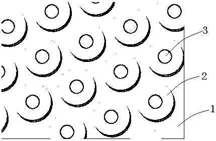
Although the existing annular oxidation step 2 is easy to process, it limits the minimum distance between adjacent light exit holes 3, which is not conducive to the integration of VCSEL arrays; moreover, this annular oxidation step 2 makes each light exit hole 3 independent, It is easy to be damaged by external force on the side; at the same time, due to the weak bonding force between the oxide layer and the non-oxide layer in the epitaxial layer, the independent ring-shaped oxidation step 2 is prone to cracking under the action of vertical stress, which affects the reliability of VCSEL.
[0003] In addition, according to the document "Control of Vertical-Cavity Laser Polarization with Anisotropic Transverse Cavity Geometries, Kent D. Choquette and R. E. Leibenguth, IEEE PHOTONICS TECHNOLOGY LETTERS, VOL. 6, NO. 1, JANUARY 1994, pp.40-42", generally The polarization of the laser emitted by the VCSEL is randomly distributed on the active layer. This characteristic is not conducive to the application of the VCSEL in the occasion where polarized light is required. The use of non-circular light holes is beneficial to improve the polarization performance of the VCSEL laser; while the existing The light exit hole produced by this ring-shaped oxidation step is circular, so it is necessary to develop a new oxidation step that can form a non-circular oxidation hole

Method used


Image

  • VCSEL chip array structure and manufacturing method thereof
  • VCSEL chip array structure and manufacturing method thereof
  • VCSEL chip array structure and manufacturing method thereof

Examples


Embodiment 1

[0033] Such as figure 2 with 3 As shown, the present embodiment provides a method for manufacturing a VCSEL chip rectangular array structure, and the specific implementation steps are as follows:

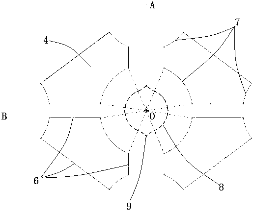
[0034] First, if figure 2As shown, the right-angled triangle AOB in the rectangular array structure of the VCSEL chip is used as the basic unit, the lengths of the two right-angled sides AO and BO of the right-angled triangle AOB are 30 microns and 40 microns respectively, and the length of the hypotenuse AB of the right-angled triangle is 50 Micron, in a right triangle, with three vertices as the center, draw three arcs 7 respectively, the radius of the arc 7 is greater than 10 microns, less than half of the shortest right angle side AO 15 microns, preferably 13 microns, three in the right triangle Short line segment 6, the short line segment parallel to the right-angled side AO of 30 microns, the distance from the parallel right-angled side AO is greater than 3 microns, prefer...

Embodiment 2

[0037] Such as Figure 4 As shown, this embodiment provides a method for manufacturing a VCSEL chip close-packed hexagonal array structure, and the specific implementation steps are as follows:

[0038] First, the equilateral triangle in the hexagonal array structure of the VCSEL chip is used as the basic unit. The length of the three sides of the equilateral triangle is 32 microns. In the equilateral triangle, with the three vertices as the center, draw three arcs respectively. The radius of the arc is greater than 10 microns, less than half of the shortest side of 16 microns, preferably 14 microns; the three short line segments in an equilateral triangle are respectively parallel to the three sides, and the distance from the parallel sides is equal, greater than 3 microns, preferably 5 microns , so that the closed polygon composed of three arcs and three short line segments makes six 60-degree rotational symmetry around any vertex of the equilateral triangle, so that six pol...


PUM

PropertyMeasurementUnit
Widthaaaaaaaaaa
Lengthaaaaaaaaaa

Abstract

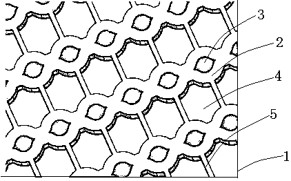
The invention provides a VCSEL chip array structure. The VCSEL chip array structure comprises a semiconductor layer, oxidation steps and holes, wherein the oxidation steps are distributed on the semiconductor layer in an array way, and are symmetrical with respect to the centers of various light-outgoing holes; each oxidation step is a polygon structure, and the adjacent oxidation steps are connected through a semiconductor rib; and oxidation holes are formed in a closed space constructed by the contour lines of multiple adjacent oxidation steps and the semiconductor rib for connecting two oxidation steps; the centers of the light-outgoing holes are symmetric and the light-outgoing holes have the non-circular oxidation front contour lines. Furthermore, the invention further provides a manufacturing method of the VSCEL chip array structure. Since the oxidation steps of the adjacent light-outgoing holes are connected through the semiconductor rib, the mechanical strength of each light-outgoing hole is guaranteed, and the oxidation steps are symmetrical with respect to the centers of various light-outgoing holes and uniformly distributed, thereby guaranteeing that the oxidation speedis uniform and symmetric along the center of each light-outgoing hole, and the light-outgoing hole is similar to circular spot, the oxidation front contour line is non-circular, and the polarization performance of the VSCEL laser can be improved.

Description

technical field [0001] The invention belongs to the technical field of semiconductor laser chip manufacturing technology, and in particular relates to a VCSEL chip array structure and a manufacturing method thereof. Background technique [0002] Vertical cavity surface emitting laser (Vertical Cavity Surface Emitting Laser, hereinafter referred to as VCSEL) since its invention in 1977, due to its low threshold current, high photoelectric conversion efficiency, single longitudinal mode output, circular spot easy to couple, array integration, easy testing , low manufacturing cost, and have been widely used in industrial fields such as optical communication, 3-D sensing infrared lighting, etc. One of the key processes of VCSEL is lateral oxidation. The oxide formed by lateral oxidation can not only effectively limit the current, but also confine the laser, thereby greatly improving the photoelectric performance of VCSEL. The usual method of lateral oxidation is to use wet etch...

Claims


Application Information

Patent Timeline
IPC IPC(8): H01S5/183
CPCH01S5/18344
Inventor 唐琦肖黎明代露
Owner 湖北光安伦芯片有限公司
Learn More