
Embedded fine circuit flexible packaging substrate and manufacturing method thereof

A manufacturing method and flexible packaging technology, which are applied in the fields of circuits, semiconductor/solid-state device manufacturing, electrical components, etc., can solve the problems of high cost and low circuit resolution, save labor hours and costs, low process cost, and simple manufacturing process. Effect

Inactive Publication Date: 2018-09-14
SHENZHEN DANBOND TECH
View PDF3 Cites 4 Cited by
  • Summary
  • Abstract
  • Description
  • Claims
  • Application Information

AI Technical Summary

Problems solved by technology

[0007] In order to overcome the deficiencies of the prior art, the present invention proposes a method of using a laser slotting method to open a micro-circuit groove on a flexible substrate to manufacture a micro-circuit flexible packaging substrate, so as to solve the problems caused by the current flexible printed circuit board manufacturing method. There are problems such as high cost and low line resolution

Method used


Image

  • Embedded fine circuit flexible packaging substrate and manufacturing method thereof
  • Embedded fine circuit flexible packaging substrate and manufacturing method thereof
  • Embedded fine circuit flexible packaging substrate and manufacturing method thereof

Examples


Embodiment 1

[0042] Embodiment 1 (continuous wire scheme)

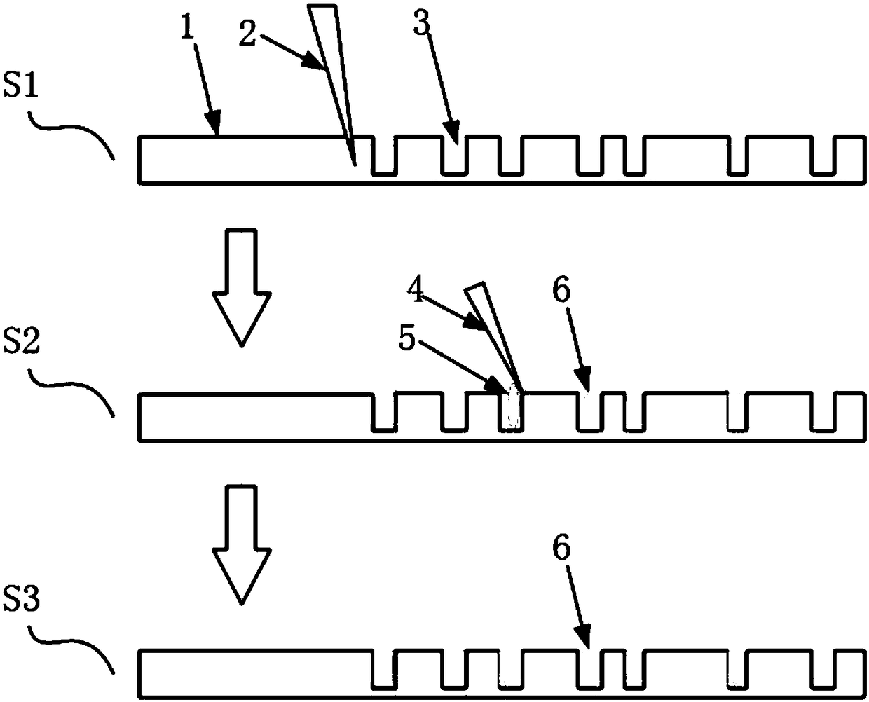
[0043] On the flexible substrate of three groups of PI film materials, the KrF gas excimer laser beam is used, and the parameters of the laser are set as follows: energy 10mJ / pulse, frequency 300Hz, reduction factor 10 times, and the atmosphere is helium, Then use the focused laser beam with set parameters to ablate continuous circuit grooves to obtain three groups of flexible substrates with circuit grooves. The circuit grooves in each group have various specifications, including those with a width of 10-100 μm. Various line widths, various line widths with a depth of 10-50μm, circuit structures such as Figure 1a shown. Next, for the three groups of flexible substrates, the three exemplary conductive pastes given in Table 1 were respectively filled, and then heated and cured by the method of the aforementioned step S3 to obtain samples. The results show that all three kinds of conductive pastes can obtain good continuous wires...

Embodiment 2

[0049] Embodiment 2 (wires interlaced with each other)

[0050] The same method as in Example 1 is used to form interlaced line grooves on the flexible substrate. The width and spacing of the line grooves include various specifications, wherein the line width includes various specifications of 10-100 μm, and the line spacing is 50, 25 , 10μm, divide the flexible substrate forming the staggered circuit trenches into two groups, and fill them with Dupont5025 and Inktec TEC-PA-10 respectively to form, for example Figure 1b Interleaved wire routing shown. figure 2 Shown is a microscopic image of a circuit structure with a line width of 10 μm and a line spacing of 25 μm filled with Dupont 5025. The four-point resistance test method is used to detect possible short circuits between wires. For Dupont 5025, for samples with a line spacing of 25 μm and above, the horizontal line-to-line resistance value is at least 20 MΩ (beyond the detection range of the measuring equipment. ). T...

Embodiment 3

[0051] Embodiment 3 (curved wire)

[0052] Use the same method as in Example 1 to ablate curved line grooves on the flexible substrate, such as 90° bends or rounded corners with different radii of curvature, and fill the three kinds of conductive pastes shown in Table 1 respectively to form, for example, Figure 1c The wire routing shown. As a concrete example, image 3 Shown is a top view micrograph of a sample filled with Dupont 5025 screen printing paste. All in all, the sharp corners, right corners and rounded corners filled by the three conductive pastes can be reliably filled, and the line width / line spacing of the lines with corners is the same as that of the straight structure.


PUM


Abstract

The invention discloses an embedded fine circuit flexible packaging substrate and a manufacturing method thereof. The manufacturing method of the embedded fine circuit flexible packaging substrate includes the following steps: S1, ablating a preset circuit groove in a flexible substrate which is made on a PI film or a PEN film by using a KrF gas excited molecular laser beam having preset technological parameters which include: energy is 10mJ / pulse, and frequency is 300Hz, and minification is 10 times and the atmosphere is helium; and under setting of the preset technological parameters, acquiring the etching rate of 0.5 mu m per pulse; S2, using a scraper blade to extrude conductive paste into the circuit groove to form a conductive circuit; and S3, drying, solidifying and cleaning the conductive circuit. The embedded fine circuit flexible packaging substrate and the manufacturing method thereof can solve the problems that the current manufacturing method flexible printed circuit boards is high in cost and is lower in the circuit resolution.

Description

technical field [0001] The invention relates to the technical field of flexible circuit boards, in particular to an embedded micro-circuit flexible packaging substrate and a manufacturing method thereof. Background technique [0002] In recent years, a new class of flexible electronics has begun to emerge, often referred to as "printed electronics". It refers to large-area, fully printed, low-cost smart electronics that have a wide range of applications in our society, such as cheap ultra-thin sensors that are attached to food packaging to detect food maturity, monitor wound healing Smart bandages, and smart active or passive RFID (radio frequency identification) tags, etc. These low-cost packages include fully printed functional logic circuits, such as conductor lines, OLEDs (organic light-emitting diodes), photodiodes, and logic circuits based on organic electronic materials; Silicon wafers with inorganic components. These products have a huge market. According to the m...

Claims


Application Information

Patent Timeline
Patent Type & Authority Applications(China)
IPC IPC(8): H01L23/12H01L21/56
CPCH01L21/56H01L23/12
Inventor 刘萍张双庆
Owner SHENZHEN DANBOND TECH
Learn More