One-dimensional material transmission electron microscopy force-electric coupling in-situ test method

A technology of transmission electron microscopy and in-situ testing, which is applied in the direction of analyzing materials, preparing test samples, and using radiation for material analysis.

Inactive Publication Date: 2020-08-14
DALIAN UNIV OF TECH
View PDF11 Cites 0 Cited by
  • Summary
  • Abstract
  • Description
  • Claims
  • Application Information

AI Technical Summary

Problems solved by technology

The traditional research method is generally to observe the material in the transmission electron microscope before and after loading, but cannot observe the change process of the material under loading in real time, so it is difficult to explain its mechanism

Method used


Image

  • One-dimensional material transmission electron microscopy force-electric coupling in-situ test method
  • One-dimensional material transmission electron microscopy force-electric coupling in-situ test method
  • One-dimensional material transmission electron microscopy force-electric coupling in-situ test method

Examples


Embodiment

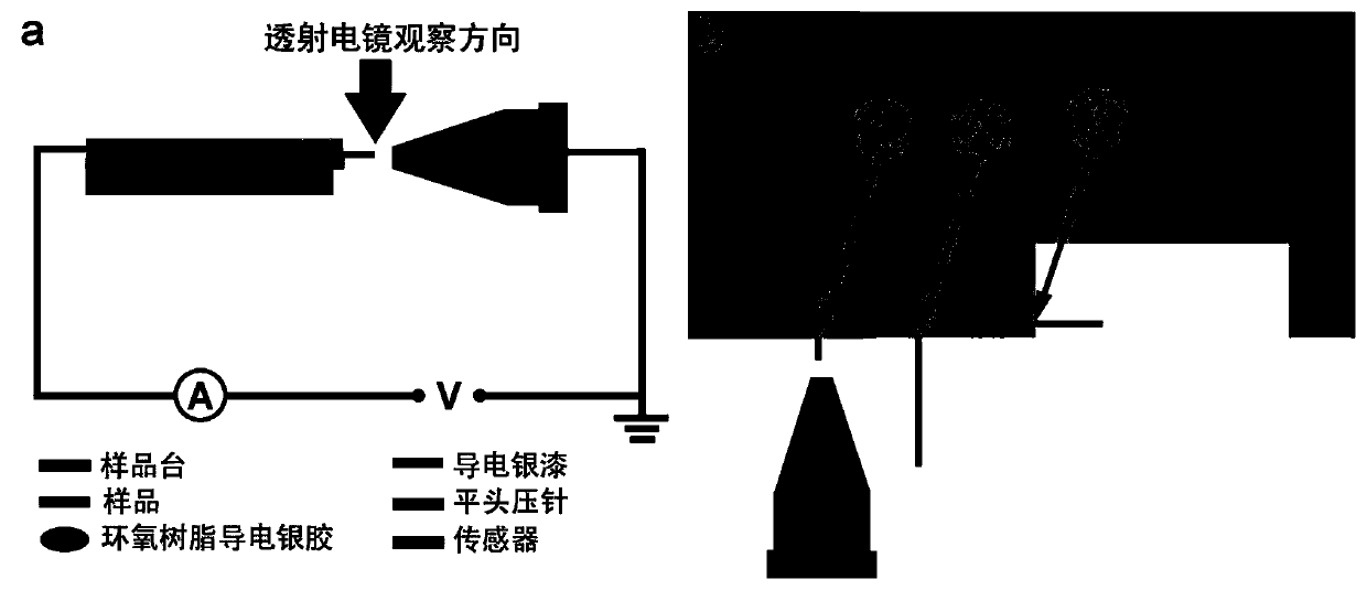
[0033] Design and process multifunctional sample stages, such as figure 1 As shown, the sample stage is processed by etching and laser stealth cutting technology on SOI chips. Its material is boron-doped P-type silicon. The overall size is 2-2.1mm long, 1.7-1.8mm wide, and 0.3-0.31mm thick. , is processed by laser stealth cutting technology; the substrate groove is 1.6-1.7mm wide and 30-40μm deep, and the substrate groove corresponding to the green square is 60-63μm wide and 20-23μm deep, and the groove is etched processed.

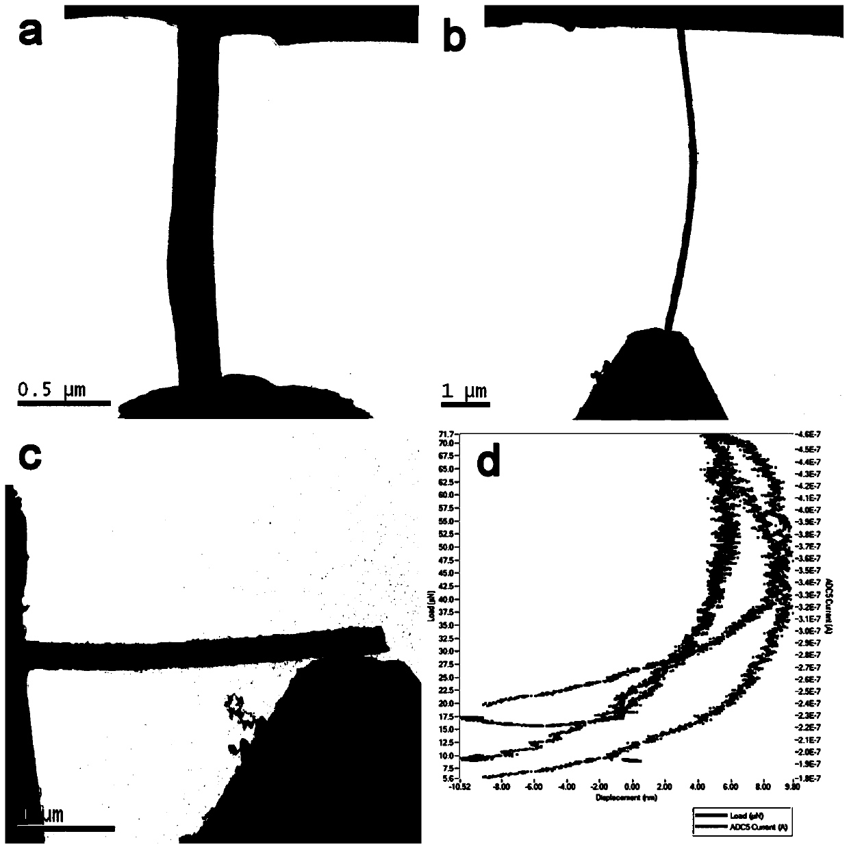
[0034] Burn the carbon film of the TEM copper grid through the inner flame of a lighter in air, and cut it in half along the center of the copper grid with a blade. The sample is a single crystal 3C-SiC nanowire with a diameter of 100-300nm and a length of 50-100μm. The sample is placed in an alcohol solution for ultrasonic dispersion for 2 minutes, and the sample is dropped on the edge of the semicircular transmission electron microscope copper grid wit...


PUM

PropertyMeasurementUnit
diameteraaaaaaaaaa
diameteraaaaaaaaaa
diameteraaaaaaaaaa

Abstract

One-dimensional material transmission electron microscopy force-electric coupling in-situ test method, design and manufacture a multifunctional sample stage that can be used to compress, buckle and bend the sample, remove the carbon film of the transmission electron microscope copper grid, and remove it through the center of the circle Cut the sample in half, ultrasonically disperse the sample in alcohol, drop the sample on the edge of the semicircular copper grid with a pipette gun, and fix a single sample on the sample stage with an epoxy resin conductive silver glue using a micromechanical device under an optical microscope The edge of the substrate, and the surface of the sample stage substrate is coated with conductive silver paint, and the force-electric coupling in-situ test is carried out in the transmission electron microscope. The invention provides a simple and efficient sample preparation and testing method for transmission electron microscope force-electric coupling in-situ observation experiment, which can carry out compression, buckling and bending experiments on samples, and can observe the material of the sample in the process of stress in real time. The change of microstructure and the change of electrical properties realize the force-electric coupling in-situ test of one-dimensional material transmission electron microscopy.

Description

technical field [0001] The invention relates to a one-dimensional material transmission electron microscope force-electricity coupling in-situ test method, in particular to a one-dimensional material in-situ nanomechanical force-electricity coupling test, and belongs to the field of transmission electron microscope in-situ nanomechanical test. Background technique [0002] With the construction and development of aviation, aerospace, deep space exploration and other projects, a series of higher requirements are put forward for the performance of high-performance equipment, and the performance of high-performance equipment depends on the performance of high-performance parts. Nanoscale surface roughness and nanoscale flatness, surface / subsurface without damage, traditional processing methods are difficult to meet this requirement, and the resulting surface / subsurface damage often affects the electrical properties of the material, thereby affecting the entire device. Performan...

Claims


Application Information

Patent Timeline
Patent Type & Authority Patents(China)
IPC IPC(8): G01N23/22G01N23/2202G01N23/2204G01N3/08G01N3/20
CPCG01N3/08G01N3/20G01N23/22G01N23/2202G01N23/2204G01N2203/0023G01N2203/0019G01N2001/364G01N1/36B82Y30/00H01J2237/2062G01N2203/0286G01N23/04G01N1/31G01N1/38G01N2001/305H01J37/261H01J2237/2802
Inventor 张振宇崔俊峰陈雷雷王博郭东明
Owner DALIAN UNIV OF TECH
Why Eureka
Try Eureka