LED lighting panel
A technology for LED lighting and LED chips, applied in electrical components, electrical solid devices, circuits, etc., can solve the problems of inability to adjust and change series and parallel, difficult to find LED chips, etc., to achieve flexible wiring, good conductivity, and avoid overflow. Effect
- Summary
- Abstract
- Description
- Claims
- Application Information
AI Technical Summary
Problems solved by technology
Method used
Image

Examples
no. 1 example
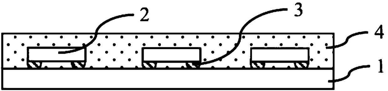
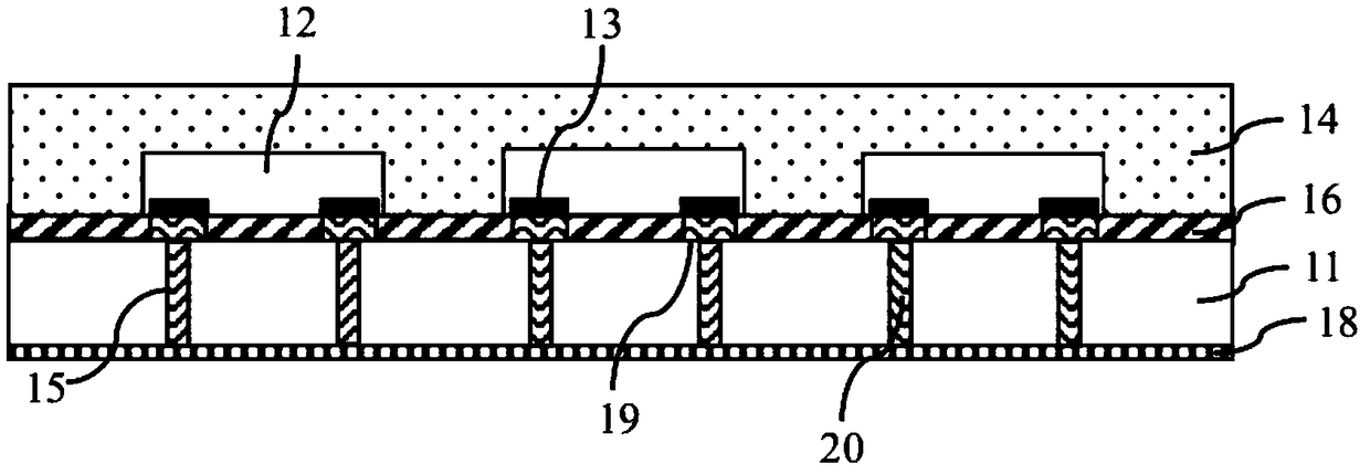
[0032] see figure 2 , the LED lighting panel of the present invention, it comprises:
[0033] an insulating substrate 11 having opposite first and second surfaces and a plurality of through holes 15 penetrating through the first and second surfaces;
[0034] The adhesive layer 16 is disposed on the first surface and has a plurality of grooves 19 corresponding to the plurality of through holes 15, and the plurality of grooves 19 are respectively connected to the plurality of through holes 15 Pass;
[0035] A plurality of LED chips 12, adhered to the adhesive layer 16, and have a plurality of electrode pads 13, the plurality of electrode pads 13 respectively correspond to the plurality of grooves 19 and in the plurality of grooves exposed in the groove 19;
[0036] encapsulating resin 14, disposed on the plurality of LED chips 12 and the bonding layer 16;
[0037] Conductive paste 20, filling the plurality of through holes 15 and the plurality of grooves 19;
[0038] The c...
no. 2 example
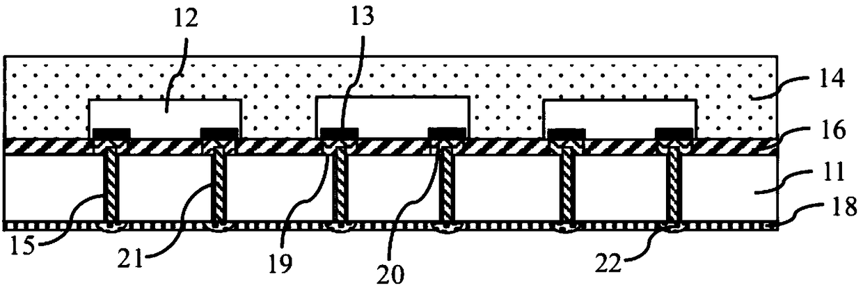
[0041] refer to image 3 , the present invention also provides another LED lighting panel, which includes:
[0042] an insulating substrate 11 having opposite first and second surfaces and a plurality of through holes 15 penetrating the first and second surfaces, and having a thickness of d1;
[0043] The adhesive layer 16 has a thickness of d2, is arranged on the first surface, and has a plurality of grooves 19 corresponding to the plurality of through holes 15, and the plurality of grooves 19 are connected to the plurality of through holes 15. The through holes 15 are respectively connected to each other;
[0044] A plurality of LED chips 12, adhered to the adhesive layer 16, and have a plurality of electrode pads 13, the plurality of electrode pads 13 respectively correspond to the plurality of grooves 19 and in the plurality of grooves exposed in the groove 19;
[0045] encapsulating resin 14, disposed on the plurality of LED chips 12 and the bonding layer 16;
[0046]...
PUM
 Abstract
Description
Claims
Application Information
 - Generate Ideas
- Intellectual Property
- Life Sciences
- Materials
- Tech Scout
- Unparalleled Data Quality
- Higher Quality Content
- 60% Fewer Hallucinations
Browse by: Latest US Patents, China's latest patents, Technical Efficacy Thesaurus, Application Domain, Technology Topic, Popular Technical Reports.
© 2025 PatSnap. All rights reserved.Legal|Privacy policy|Modern Slavery Act Transparency Statement|Sitemap|About US| Contact US: help@patsnap.com