Power semiconductor device with wave type field limiting ring structure and preparation method of device

A power semiconductor, wave-type technology, applied in semiconductor/solid-state device manufacturing, semiconductor devices, electrical components, etc., can solve problems affecting device robustness, device failure, dynamic avalanche, etc., to suppress dynamic avalanche and reduce surface electric field Effect

Inactive Publication Date: 2018-09-07
SOUTHEAST UNIV +1
View PDF6 Cites 3 Cited by
  • Summary
  • Abstract
  • Description
  • Claims
  • Application Information

AI Technical Summary

Problems solved by technology

These power semiconductor devices need to realize high-frequency switching under high-voltage and high-current conditions, and often induce dynamic avalanche when the high-current is turned off, that is, when the power semiconductor device transitions from the forward conduction state to the reverse bias state, resulting in Device failure, affecting the robustness of the device

Method used


Image

  • Power semiconductor device with wave type field limiting ring structure and preparation method of device
  • Power semiconductor device with wave type field limiting ring structure and preparation method of device
  • Power semiconductor device with wave type field limiting ring structure and preparation method of device

Examples


Embodiment Construction

[0031] The present invention will be described in detail below with reference to the drawings.

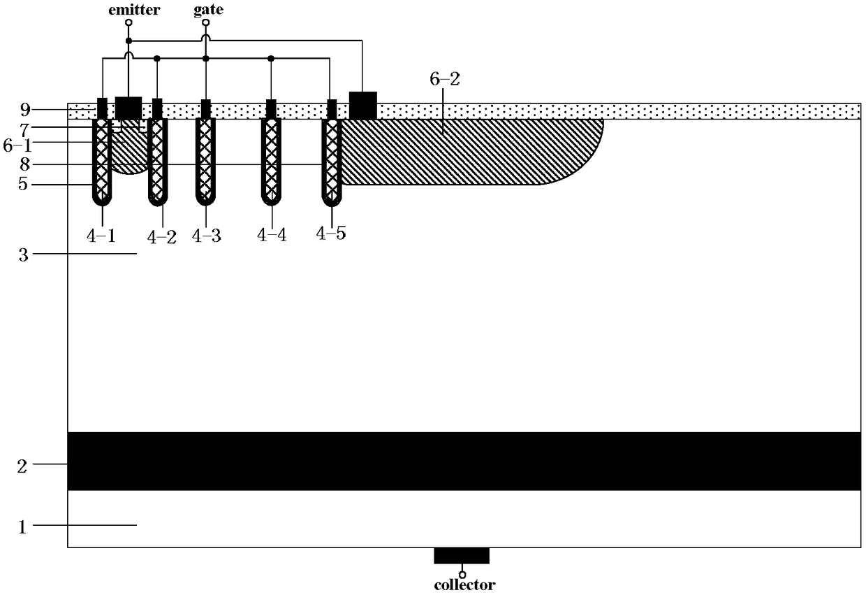
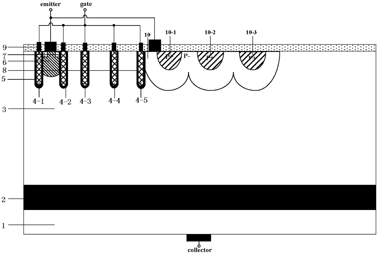
[0032] Reference figure 2 , To explain the present invention in detail, a power semiconductor device with a wave-shaped field limiting ring structure and a preparation method thereof, comprising: a P-type substrate 1, and an anode metal layer is provided at the bottom of the P-type substrate 1 as The collector of the device is provided with an N-type buffer layer 2 above the P-type substrate 1, an N-type epitaxial layer 3 is provided on the N-type buffer layer 2, and the N-type epitaxial layer 3 is divided into a cell area and a transition area And the terminal area, a field oxide layer 9 is provided on the N-type epitaxial layer 3, two cell area gate trenches 4-1, 4-2 are provided in the cell area, and three transition areas are provided in the transition area The gate trenches 4-3, 4-4, 4-5 are provided with a P-type body region 6 between the gate trenches 4-1, 4-2 of the two cell ...


PUM


Abstract

The invention relates to a power semiconductor device with a wave type field limiting ring structure. The device comprises a P-type substrate (1). An N-type buffer layer (2) is arranged on the P-typesubstrate (1). An N-type epitaxial layer (3) is arranged on the N-type buffer layer (2). The N-type epitaxial layer (3) is divided into a cell region, a transition region, and a termination region. Gate trenches (4-1) and (4-2) are formed in the cell region. Gate trenches (4-3), (4-4) and (4-5) are formed in the transition region. A P-type body region (6) is arranged between the gate trenches (4-1) and (4-2). A heavily doped N-type emitter (7) is arranged in the P-type body region (6). The device is characterized in that a wave-type overlapped ion diffusion region (10) is arranged in the terminal region; and ion implantation regions (10-1), (10-2) and (10-3) are arranged in the wave-type ion diffusion region (10). The device structure of the present invention is capable of suppressing electric field spikes generated when the device is turned off, thereby suppressing dynamic avalanche.

Description

Technical field [0001] The present invention mainly relates to the technical field of power semiconductor devices, in particular to a power semiconductor device with a wave-shaped field limiting loop structure and a preparation method thereof. The power semiconductor device is mainly used in the fields of high-power motor transmission, locomotive traction and high-voltage power transmission. Background technique [0002] Power semiconductor devices have the advantages of high blocking voltage, reduced conduction voltage, simple driving circuit, good controllability and large safe working area. Power semiconductor devices are widely used in various energy conversion systems, such as power transmission systems (high-voltage direct current transmission and wireless power transmission), transportation systems (railroads, maglev trains, and aerospace), and industrial drive systems (variable speed drives). With the rapid development of industrial variable speed drive technology, more a...

Claims


Application Information

Patent Timeline
IPC IPC(8): H01L29/06H01L29/739H01L21/331
CPCH01L29/0684H01L29/66348H01L29/7397H01L29/7398
Inventor 孙伟锋张小双童鑫吴其祥刘斯扬陆生礼时龙兴
Owner SOUTHEAST UNIV
Why Eureka
Try Eureka