
Dielectric geometric phase metasurface material with low depth-to-width ratio and structural optimization method thereof

A dielectric and metasurface technology, applied in the field of micro-nano optics, can solve the problems of inability to guarantee device yield and mass production, inability to guarantee minimum process error requirements, lack of development ideas, etc., achieving continuous geometric phase adjustment function, easy to promote The effect of production, yield and mass production assurance

Inactive Publication Date: 2018-09-04
WUHAN UNIV
View PDF6 Cites 34 Cited by
  • Summary
  • Abstract
  • Description
  • Claims
  • Application Information

AI Technical Summary

Problems solved by technology

However, although scientists claim that the metasurface process is fully compatible with existing semiconductor processes, in fact its manufacturing is constantly challenging the limits of current semiconductor process processing, and there is even a lack of effective development ideas in terms of mass production.
For example, the titanium dioxide metasurface lens, which was rated as one of the top ten technological breakthroughs in the world in 2016 by Science magazine, has a micro-nano structure with an aspect ratio as high as 15. [1] , the traditional semiconductor process cannot guarantee the required minimum process error requirements
Even if the atomic layer deposition (ALD) process mentioned in the article is adopted, the yield and mass production of the device are still not guaranteed, not to mention the performance of high aspect ratio devices in terms of imaging vignetting and off-axis point aberration correction also unsatisfactory

Method used


Image

  • Dielectric geometric phase metasurface material with low depth-to-width ratio and structural optimization method thereof
  • Dielectric geometric phase metasurface material with low depth-to-width ratio and structural optimization method thereof
  • Dielectric geometric phase metasurface material with low depth-to-width ratio and structural optimization method thereof

Examples


Embodiment Construction

[0039] In order to illustrate the present invention and / or the technical solutions in the prior art more clearly, the embodiments of the present invention will be described below with reference to the accompanying drawings. Obviously, the drawings in the following description are only some embodiments of the present invention, and those skilled in the art can obtain other drawings based on these drawings and obtain other implementations.

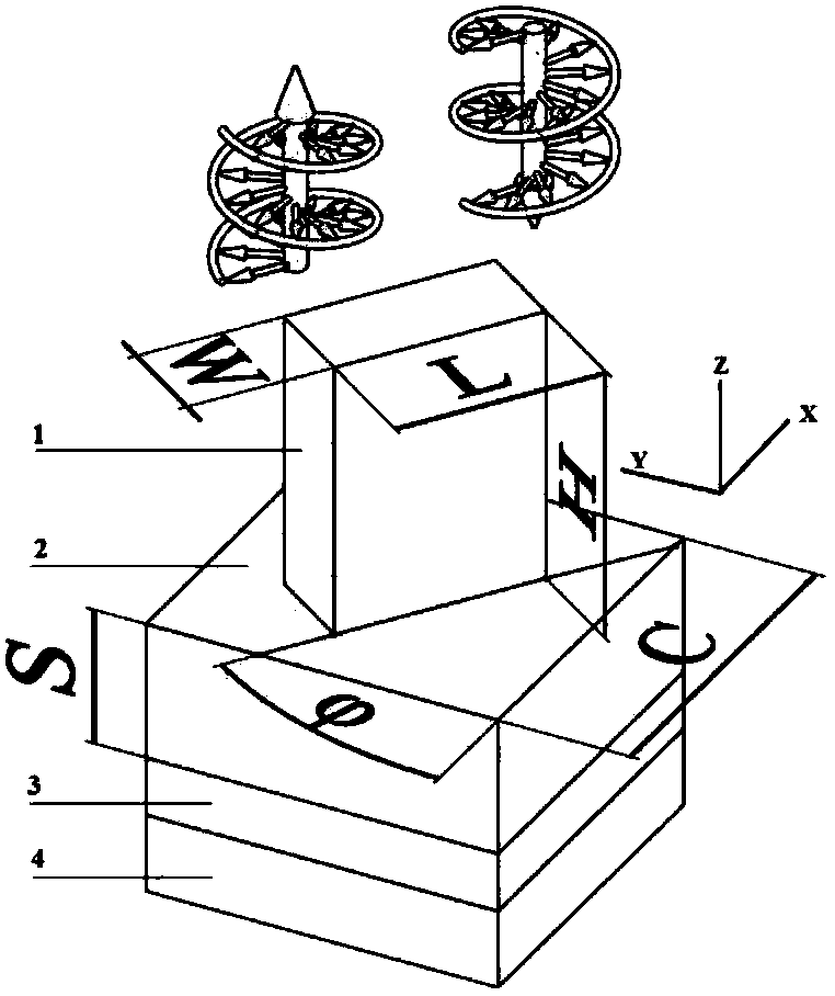
[0040] see figure 1 , is shown as a structural schematic diagram of the dielectric geometric phase metasurface material of the present invention, the dielectric geometric phase metasurface material shown includes a substrate 4, a reflective layer 3 on the substrate 4, an F-P layer 2 on the reflective layer 3, and an F-P layer arranged on the F-P The dielectric nano-brick array on the layer 2 is composed of a number of dielectric nano-bricks 1 uniformly arranged in the same size, and the dielectric nano-brick 1 is in the shape of a cuboid. ...


PUM


Abstract

The invention discloses a dielectric geometric phase metasurface structure material with a low depth-to-width ratio and a structural optimization method thereof. The dielectric geometric phase metasurface structure material comprises a substrate, a reflecting layer on the substrate, a multi-beam interference layer on the reflecting layer and a dielectric nano brick array formed by periodically arranging a plurality of dielectric nano bricks with consistent sizes on the multi-beam interference layer, wherein the dielectric nano brick array is used for receiving perpendicularly incident circularly polarized light and adjusting the phase of the emergent light through adjusting the direction of each dielectric nano brick. The depth-to-width ratio of the dielectric geometric phase metasurface structure material is reduced to half of the depth-to-width ratio of the traditional transmission-type metasurface material, and the depth-to-width ratio is about 1.7, so that the requirements for theprocessing technology are reduced, and the finished product rate and mass production of the device are guaranteed.

Description

technical field [0001] The invention relates to the field of micro-nano optics, in particular to a dielectric geometric phase metasurface material with a low aspect ratio and a structure optimization method thereof. Background technique [0002] In recent years, a new generation of artificial electromagnetic structural materials represented by metasurfaces has become a hot spot in many fields. As the unique optical properties of metasurfaces and many novel physical phenomena are continuously discovered, the industry is eagerly looking forward to its ability to lead a new round of optoelectronic industry revolution. However, although scientists claim that the metasurface process is fully compatible with existing semiconductor processes, in fact its manufacturing is constantly challenging the limits of current semiconductor process processing, and there is even a lack of effective development ideas in terms of mass production. For example, the titanium dioxide metasurface len...

Claims


Application Information

Patent Timeline
IPC IPC(8): G02B1/00G02F1/01
Inventor 郑国兴邓娟陶金武霖刘子晨邓联贵戴琦付娆李子乐刘勇毛庆洲李松
Owner WUHAN UNIV
Learn More