Organic light-emitting display panel, display device and preparation method thereof
An organic light-emitting panel and light-emitting display technology, which is applied in semiconductor/solid-state device manufacturing, electrical components, electric solid-state devices, etc., can solve the problems of material and device life attenuation, so as to improve life, improve utilization rate, and increase number density Effect
- Summary
- Abstract
- Description
- Claims
- Application Information
AI Technical Summary
Problems solved by technology
Method used
Image

Examples
Embodiment 1
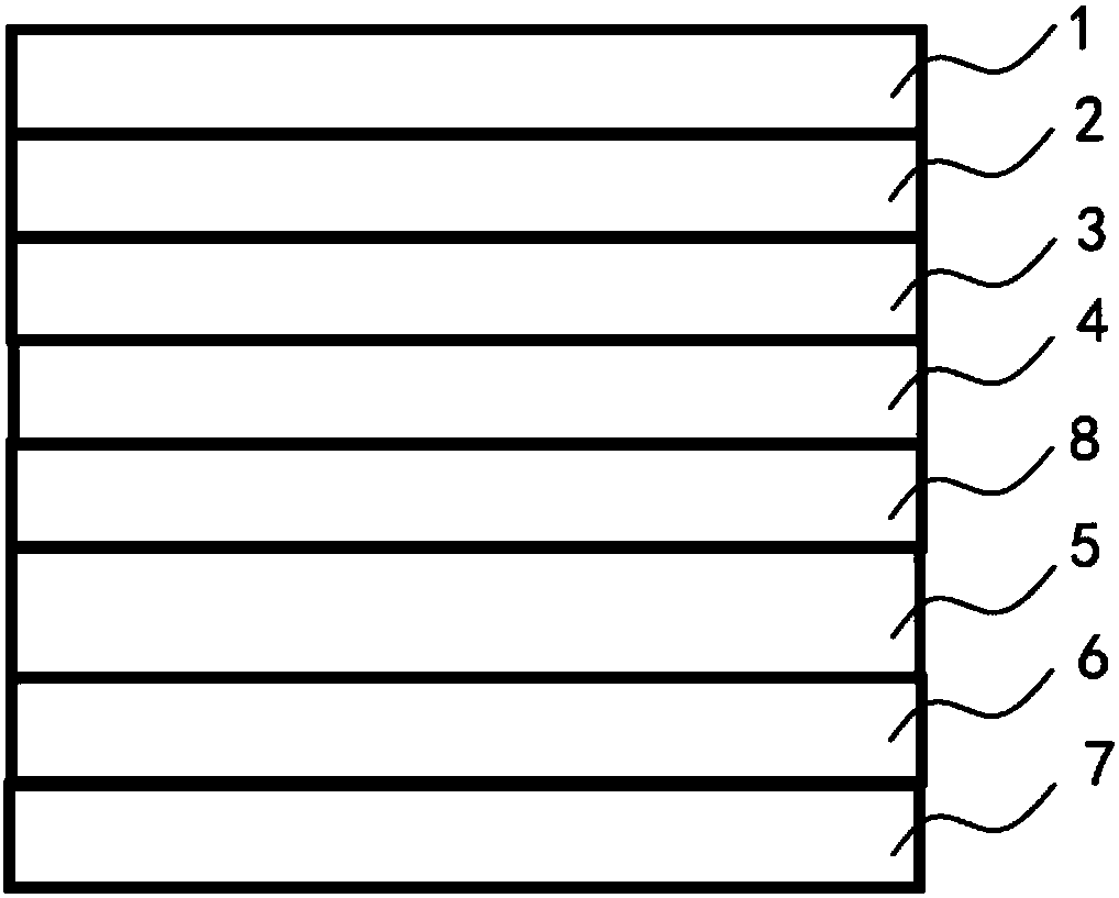
[0040] Using the indium tin oxide (ITO) layer on the substrate as the anode, sequentially form the hole injection layer (5-30nm), the hole transport layer (1000-1300nm), the first electron blocking layer (10-80nm), and the light-emitting layer (20~40nm), electron transport layer (20~35nm), electron injection layer (1~3nm), Mg-Ag alloy cathode.
[0041] The doping material is m-MTADATA.
Embodiment 2
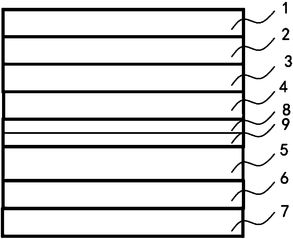
[0043]Using the indium tin oxide ITO layer on the substrate as the anode, sequentially form the hole injection layer (5-30nm), the hole transport layer (1000-1300nm), the second electron blocking layer (5-70nm), the first electron blocking layer layer (5-10nm), light-emitting layer (20-40nm), electron transport layer (20-35nm), EIL (1-3nm), Mg-Ag alloy cathode.
[0044] Doping material is Ir(ppy) 3 .
[0045] The present invention improves the lifetime of the inventive device by doping or partially doping (adjacent to the EBL / EML interface) hole-type dopant material in the EBL. The reason why the lifetime can be improved is that the electron blocking layer itself is generally an electron-rich material, and generally contains an aniline structure. The recombination interface is between EBL / EML, which means that a large number of electrons will be transmitted to this interface, if the transported electrons cannot be recombined by holes in time. Then too many electrons will ha...
PUM
 Abstract
Description
Claims
Application Information
 - R&D
- Intellectual Property
- Life Sciences
- Materials
- Tech Scout
- Unparalleled Data Quality
- Higher Quality Content
- 60% Fewer Hallucinations
Browse by: Latest US Patents, China's latest patents, Technical Efficacy Thesaurus, Application Domain, Technology Topic, Popular Technical Reports.
© 2025 PatSnap. All rights reserved.Legal|Privacy policy|Modern Slavery Act Transparency Statement|Sitemap|About US| Contact US: help@patsnap.com