
Optical component surface profile processing process and parameter selection method and application method thereof

A technology for optical components and parameter selection, applied in special data processing applications, electrical digital data processing, instruments, etc., can solve problems such as suboptimal, and achieve the effect of improving accuracy, avoiding manual judgment, and quickly converging parameter selection.

Active Publication Date: 2018-08-24
NAT UNIV OF DEFENSE TECH
View PDF5 Cites 5 Cited by
  • Summary
  • Abstract
  • Description
  • Claims
  • Application Information

AI Technical Summary

Problems solved by technology

This method works, but is not optimal

Method used


Image

  • Optical component surface profile processing process and parameter selection method and application method thereof
  • Optical component surface profile processing process and parameter selection method and application method thereof
  • Optical component surface profile processing process and parameter selection method and application method thereof

Examples


Embodiment Construction

[0024] The following will take a Φ540mm SiC off-axis aspheric mirror as an example to further explain the process, parameter selection and application method of the surface shape processing of the optical element of the present invention.

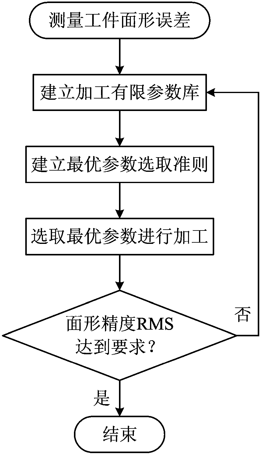
[0025] Such as figure 1 As shown, the implementation steps of the process and parameter selection method of optical element surface processing in this embodiment include:

[0026] 1) Establishing a processing limited parameter library for the target optical component, the processing limited parameter library includes at least two or more groups of processes and parameters for surface processing of the target optical component;

[0027] 2) Calculate the modification efficiency FA of each group of processes and parameters;

[0028] 3) Select a group of processes and parameters with the largest modification efficiency FA value as the output optimal process and parameters.

[0029] In the present embodiment, in step 2), the functional express...


PUM


Abstract

The invention discloses an optical component surface profile processing process and parameter selection method and an application method thereof. The process and parameter selection method comprises the implementation steps of establishing a processing finite parameter library for a target optical component; calculating shape correction efficiency FA of each group of processes and parameters; andselecting a group of processes and parameters with a maximum shape correction efficiency FA value as output optimal processes and parameters. The application method of the process and parameter selection method comprises the implementation steps of determining optimal processes and parameters; and according to the optimal processes and parameters, performing surface profile iterative processing onthe target optical component until the surface profile precision of the target optical component meets a specified condition. The manual misjudgment can be avoided; process route establishment of efficient and high-precision processing of the optical component is realized; and through an optimal parameter selection criterion, the processes and parameters most suitable for current surface profileare objectively and comprehensively evaluated, so that the uncertainty and non-objectivity of manual process selection are avoided and the process selection accuracy is effectively improved.

Description

technical field [0001] The invention relates to the polishing technology of optical parts, in particular to a process and parameter selection of surface shape processing of optical elements and an application method thereof. Background technique [0002] According to the diffraction theory of optics, increasing the aperture of the optical system is an effective means to improve the resolution of the system. With the development of optical technology, the optical components used in the new generation of optical systems have higher and higher requirements for surface accuracy, which puts forward higher requirements for optical processing technology. The processing of high-precision optical components is a complicated and lengthy process, and its technological process includes: milling and forming, CNC grinding, rough polishing, fine polishing, etc. The processing of high-precision optical components cannot be completed by relying on a single process or polishing tool. How to ...

Claims


Application Information

Patent Timeline
Patent Type & Authority Applications(China)
IPC IPC(8): G06F17/50B24B1/00
CPCB24B1/00G06F30/20
Inventor 宋辞戴一帆彭小强杜航石峰胡皓
Owner NAT UNIV OF DEFENSE TECH
Learn More