Superconducting wire rod
A technology of superconducting wire and superconducting material, applied in the field of superconducting wire, can solve the problem that the ceramic layer cannot generate stress and so on
- Summary
- Abstract
- Description
- Claims
- Application Information
AI Technical Summary
Problems solved by technology
Method used
Image

Examples
specific Embodiment approach
[0049] Embodiments of the present invention will be described below based on the drawings. In the following drawings, the same or corresponding parts are denoted by the same reference numerals, and description thereof will not be repeated.
no. 1 example
[0051] Construction of Superconducting Wires
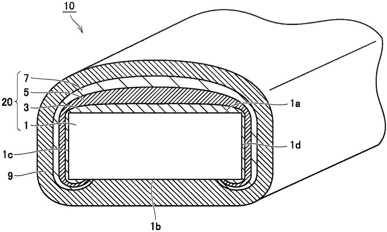
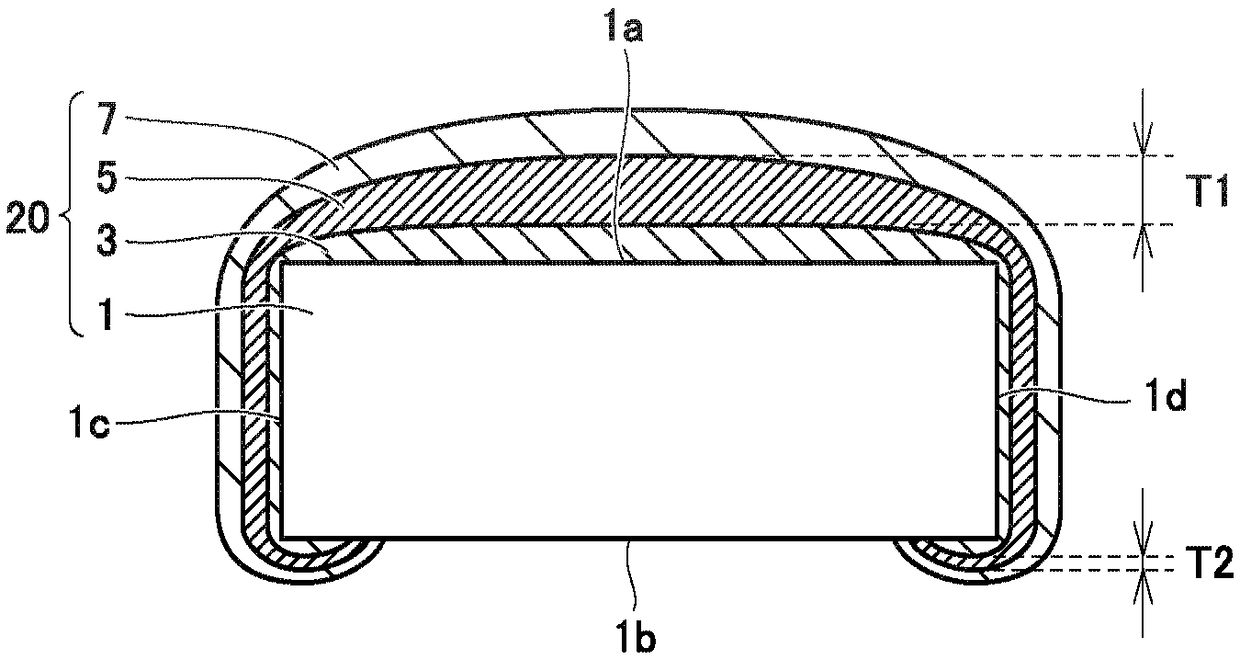
[0052] figure 1 is a schematic cross-sectional view showing the configuration of the superconducting wire in the first embodiment. figure 1 A section in a direction transverse to the direction in which superconducting wire 10 extends in the first embodiment is shown. Therefore, the direction transverse to the plane of the drawing is the longitudinal direction of the superconducting wire, and the superconducting current in the layer 5 of superconducting material flows in the direction transverse to the plane of the drawing. In addition, in figure 1 And in the schematic cross-sectional views in subsequent figures, in order to facilitate easy recognition of the drawings, the distance between the dimension in the vertical direction (hereinafter also referred to as "thickness direction") and the dimension in the left-right direction (hereinafter also referred to as "width direction") is shown. The difference is small. However, in r...
no. 2 example
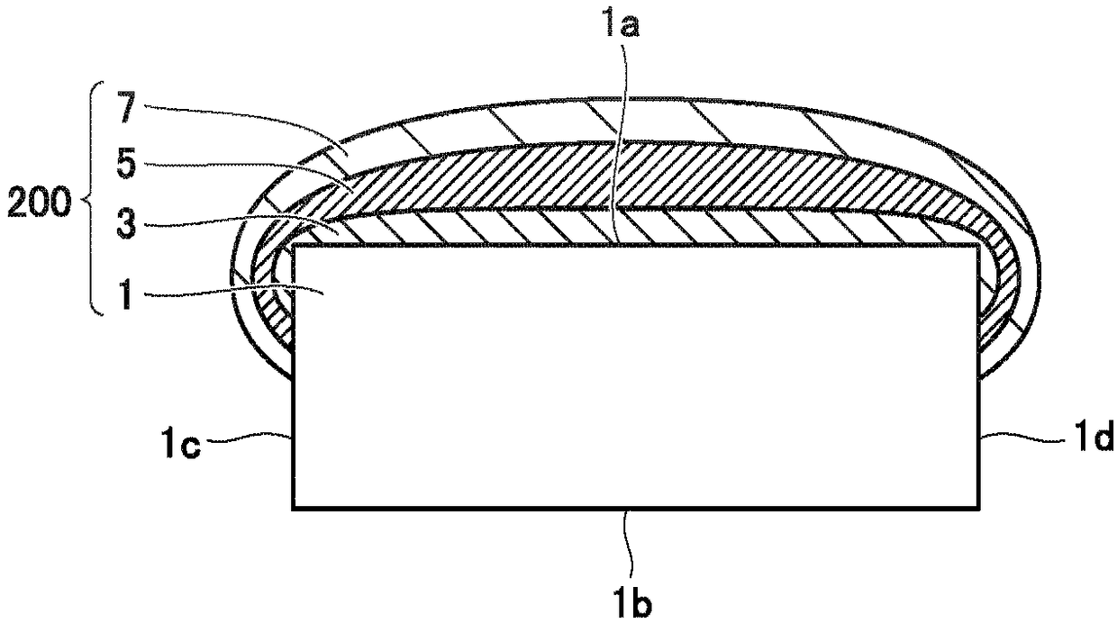
[0109] Figure 11 is a schematic cross-sectional view showing the configuration of a superconducting wire 10C in the second embodiment. Figure 11 A cross section in a direction transverse to the direction in which superconducting wire 10C extends is shown.
[0110] refer to Figure 11 , except that the structure of the multilayer stack 20 differs from figure 2 In addition to the structure of the multilayer stack 20 shown, basically the superconducting wire 10C in the second embodiment has the same figure 1 The superconducting wire 10 shown has a similar structure.
[0111] In the superconducting wire 10C, the intermediate layer 3, the superconducting material layer 5, and the protective layer 7 on the first main surface 1a protrude at opposite ends in the width direction, respectively, and thus have a central portion retracted in the width direction thereof. section. In other words, the upper surface of each of intermediate layer 3 , superconducting material layer 5 and...
PUM
| Property | Measurement | Unit |
|---|---|---|
| Thickness | aaaaa | aaaaa |
| Thickness | aaaaa | aaaaa |
Abstract
Description
Claims
Application Information
 - R&D
- Intellectual Property
- Life Sciences
- Materials
- Tech Scout
- Unparalleled Data Quality
- Higher Quality Content
- 60% Fewer Hallucinations
Browse by: Latest US Patents, China's latest patents, Technical Efficacy Thesaurus, Application Domain, Technology Topic, Popular Technical Reports.
© 2025 PatSnap. All rights reserved.Legal|Privacy policy|Modern Slavery Act Transparency Statement|Sitemap|About US| Contact US: help@patsnap.com