Pressure sensor package structure and package method

A pressure sensor and packaging structure technology, applied in microstructure devices, manufacturing microstructure devices, microstructure technology, etc., can solve the problem of affecting pressure transmission, uneven contact between flexible colloid and cavity, and inability to effectively maintain product shape. Chip protection and other issues, to achieve excellent performance and ensure the effect of surface flatness

Pending Publication Date: 2018-07-27
山东盛芯电子科技有限公司
View PDF0 Cites 0 Cited by
  • Summary
  • Abstract
  • Description
  • Claims
  • Application Information

AI Technical Summary

Problems solved by technology

[0002] The sensor package used to measure pressure needs to be potted with flexible colloid for protection and to be able to transmit pressure. For example, the pressure sensor used to measure pulse does not have a cavity support around the sensor. Due to the low hardness of the flexible colloid, it cannot be effectively maintained. The shape of the product protects the gold wire and chip inside the product. If a cavity support is designed around the sensor, after the flexible colloid is potted, the surrounding walls play a supporting role and affect the pressure transmission.
In addition, due to the tension on the surface of the colloid, there is unevenness in the contact between the flexible colloid and the cavity after normal curing.

Method used


Image

  • Pressure sensor package structure and package method
  • Pressure sensor package structure and package method
  • Pressure sensor package structure and package method

Examples


Embodiment Construction

[0026] The present invention will be further described below in conjunction with the accompanying drawings and embodiments.

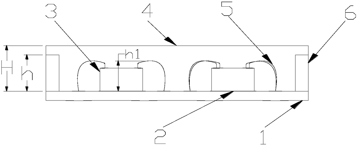
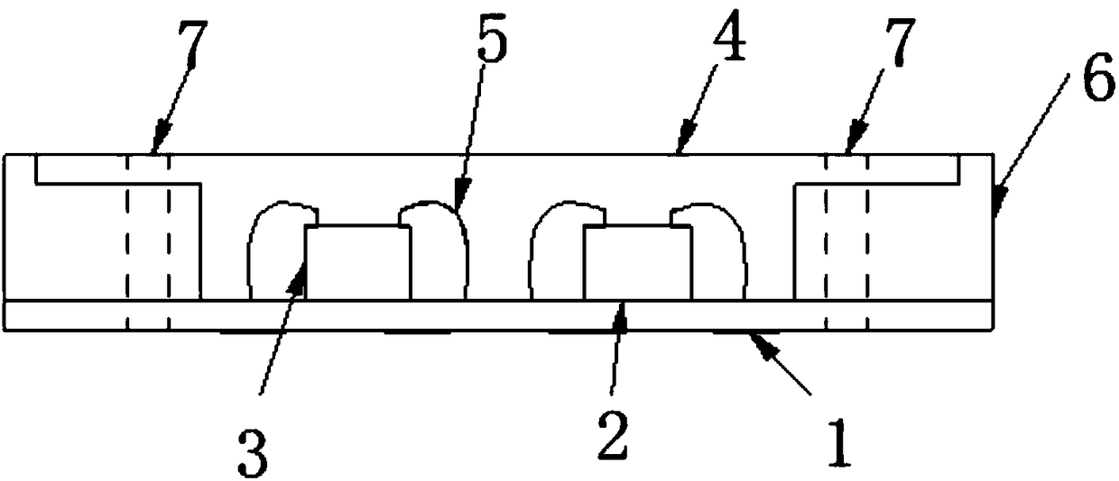
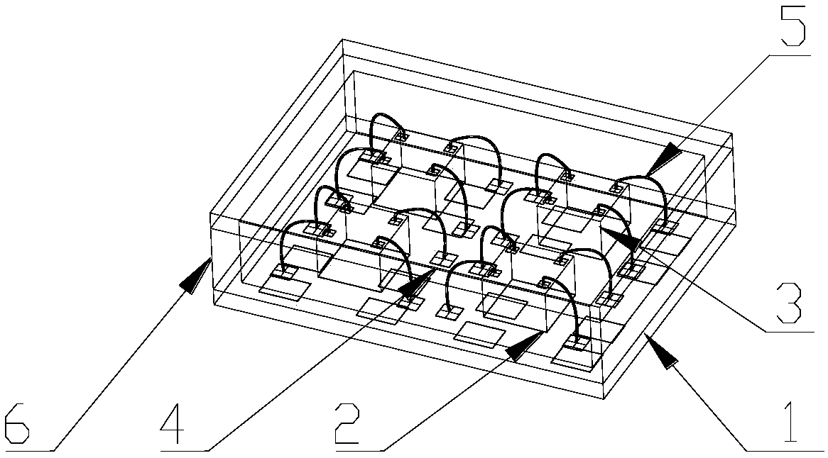
[0027] like figure 1 As shown, a pressure sensor packaging structure, the pressure sensor in this embodiment is a pressure sensor for pulse measurement, including a packaging substrate 1, including a rigid colloid 6 on the packaging substrate, and the rigid colloid 6 is arranged around the packaging substrate 1 , enclosing a cavity, the cavity is provided with a chip 3, the chip is pasted on the package substrate through the adhesive 2, the pad of the chip is connected with the pad of the package substrate through the gold wire 5, and the gold wire forms an arc shape; the cavity and the upper surface of the rigid colloid are filled with flexible colloid 4.

[0028] The distance from the top surface of the flexible colloid to the packaging substrate is H, the distance from the top surface of the rigid colloid to the packaging substrate is h, the distanc...


PUM


Abstract

The invention discloses a pressure sensor package structure and package method. The structure comprises a package substrate, the edge of the package substrate is provided with a circle of rigid colloid, a hollow cavity is formed in the rigid colloid, a chip is arranged in the hollow cavity, a bonding pad of the chip is connected to the bonding pad of the package substrate through a gold wire, andthe gold wire is curved; the interior of the hollow cavity and the upper surface of the rigid colloid are filled with the flexible colloid; the distance from the top surface of the flexible colloid tothe package substrate is H, the distance from the top surface of the rigid colloid to the package substrate is h, the distance from the vertex of the gold wire to the package substrate is h1, and H>h>h1 is satisfied. The chip is pasted onto the package substrate by adhesive bonding. The pressure sensor package structure disclosed by the invention not only ensures the shape regularity of the product but also has the rigidity to achieve the purpose of protecting the chip and the gold wire in the case of ensuring the excellent performance of the pressure sensor, and the surface flatness of the potting colloid is ensured by a process method.

Description

technical field [0001] The invention relates to the technical field of semiconductor packaging, in particular to a pressure sensor packaging structure and packaging method. Background technique [0002] The sensor packaging used to measure pressure needs to be potted with flexible colloid for protection and pressure transmission. For example, the pressure sensor used to measure pulse does not have a cavity around the sensor. Due to the low hardness of the flexible colloid, it cannot be effectively maintained. The shape of the product protects the gold wire and chip inside the product. If a cavity support is designed around the sensor, after the flexible colloid is potted, the surrounding walls will play a supporting role and affect the pressure transmission. In addition, due to the tension on the surface of the colloid, there will be unevenness in the contact between the flexible colloid and the cavity after normal curing. Contents of the invention [0003] The purpose of...

Claims


Application Information

Patent Timeline
Patent Type & Authority Applications(China)
IPC IPC(8): B81B3/00B81C1/00A61B5/02
CPCA61B5/02B81B3/0027B81C1/00261B81C1/00269
Inventor 刘昭麟邢广军
Owner 山东盛芯电子科技有限公司
Why Eureka
Try Eureka