IC card
A technology of insulating substrates and chips, applied in printing, instruments, electrical components, etc., can solve problems such as unsatisfactory elimination of deformation of reinforcing sheets, uneven surface of card substrates, heating of heat-sensitive recording layers, etc.
- Summary
- Abstract
- Description
- Claims
- Application Information
AI Technical Summary
Problems solved by technology
Method used
Image
Examples
example 1
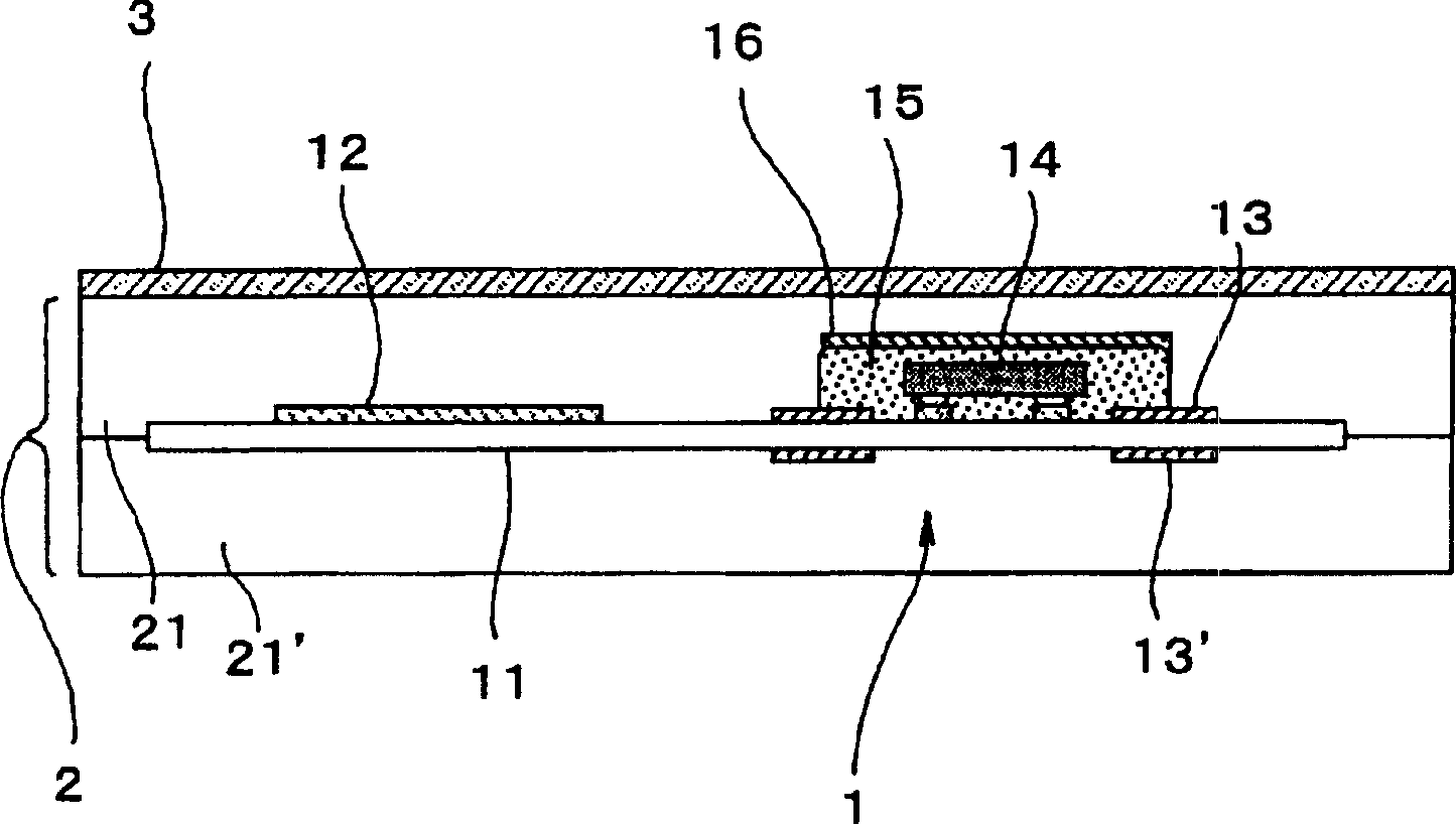
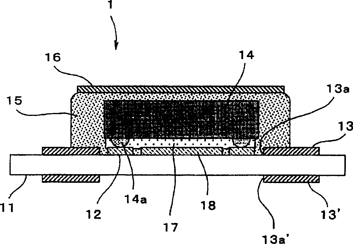
[0108] In the IC card of Example 1, the Figure 10 The IC module 1 shown in plan view (viewed from the top of the reinforcement sheet 16, this also applies to subsequent views) in which the reinforcement film pattern 13 is provided only on the IC mounting surface. The reinforcing film pattern 13 is a square, and the length of one side is 0.5 mm shorter than the diameter of the reinforcing sheet 16, that is, a square whose outer periphery is 6.5 mm×6.5 mm. In addition, in the reinforcing film pattern 13, the shape of the opening 13a is a square, and the length of one side is 0.3mm longer than the side of the square IC chip 14, that is, the shape of the opening 13a is a square of 4.3mm×4.3mm. The outer sides of the reinforcing film pattern 13 are parallel to the corresponding sides of the opening 13a. Furthermore, the reinforcement film pattern 13 can be obtained by forming a pattern in the same conductive film as that used for the circuit pattern 12, so that a bypass is formed...
example 2
[0111] In the IC card of example 2, used such as Figure 11 In the shown IC module, the reinforcing film patterns 13, 13' are respectively provided on the IC mounting surface and the non-mounting surface. The shape and structure of the reinforcement film pattern 13 on the mounting surface of the IC chip 14 and the reinforcement sheet 16 are the same as those in Example 1. The reinforcing film pattern 13' on the non-mounting surface has the same outer peripheral shape as that of the reinforcing film pattern 13 on the mounting surface and has an opening 13a'. No bypass pattern is formed at the portion where the circuit pattern 12 is formed in the reinforcing film pattern 13', and only a square opening 13a' is formed in the center of the square pattern in the same direction.
[0112] The reinforcing film pattern 13, the IC chip 14, the reinforcing sheet 16 and the reinforcing film pattern 13' having the above-mentioned shape are arranged so that the IC chip 14 is arranged in the...
example 3
[0114] In the IC card of example 3, used such as Figure 12 In the IC module shown in , wherein the reinforcing film pattern 13' is provided only on the non-mounting surface of the IC chip 14. The structures of the IC chip 14, the reinforcement sheet 16 and the reinforcement film pattern 13' are the same as in Example 2.
PUM
 Abstract
Description
Claims
Application Information
 - R&D
- Intellectual Property
- Life Sciences
- Materials
- Tech Scout
- Unparalleled Data Quality
- Higher Quality Content
- 60% Fewer Hallucinations
Browse by: Latest US Patents, China's latest patents, Technical Efficacy Thesaurus, Application Domain, Technology Topic, Popular Technical Reports.
© 2025 PatSnap. All rights reserved.Legal|Privacy policy|Modern Slavery Act Transparency Statement|Sitemap|About US| Contact US: help@patsnap.com


