Production method of PCB (printed circuit board) and PCB

A production method and graphic technology, which is applied in the direction of multilayer circuit manufacturing, printed circuit manufacturing, conductive pattern layout details, etc., can solve the problems affecting the performance and assembly of the circuit graphic layer, uneven surface, layered blistering, etc., to achieve maintenance Surface flatness and solderability, smooth coating, and enhanced bonding effect

Pending Publication Date: 2018-06-29
SHENZHEN TONGWEIXIN CIRCUIT TECH CO LTD
View PDF0 Cites 0 Cited by
  • Summary
  • Abstract
  • Description
  • Claims
  • Application Information

AI Technical Summary

Problems solved by technology

[0003] However, due to the thick copper and board thickness of the PCB for charging piles, when the temperature increases sharply, the PCB for charging piles is prone to a series of reliability problems such as layered blistering and copper surface warping, resulting in uneven surfaces. , affecting the performance and assembly of the line graphics layer

Method used


Image

  • Production method of PCB (printed circuit board) and PCB
  • Production method of PCB (printed circuit board) and PCB

Examples


Embodiment 2

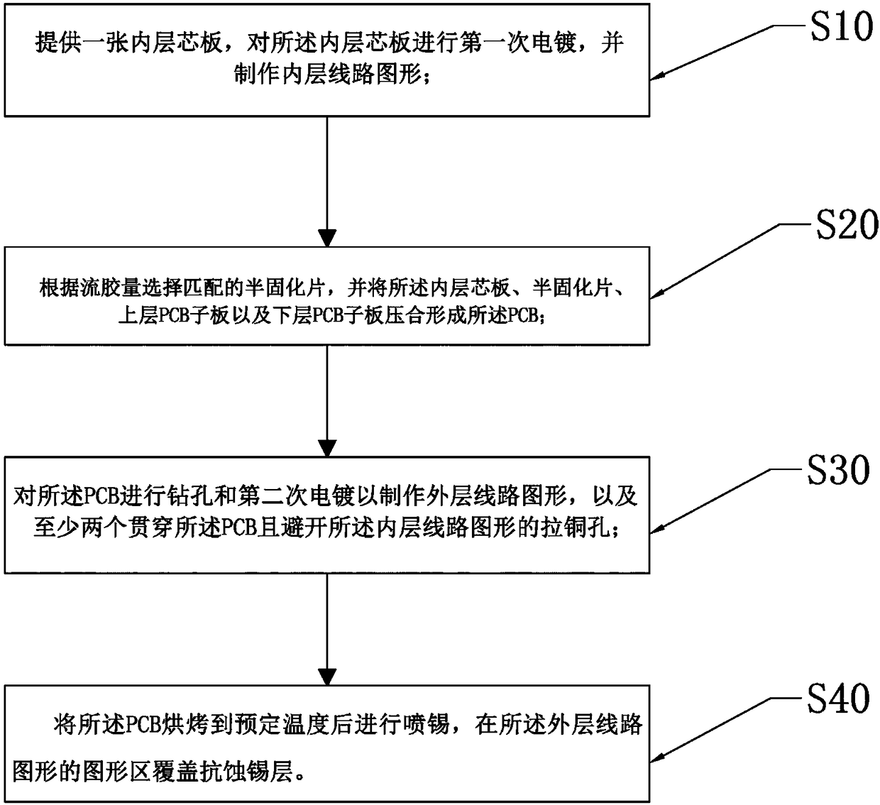
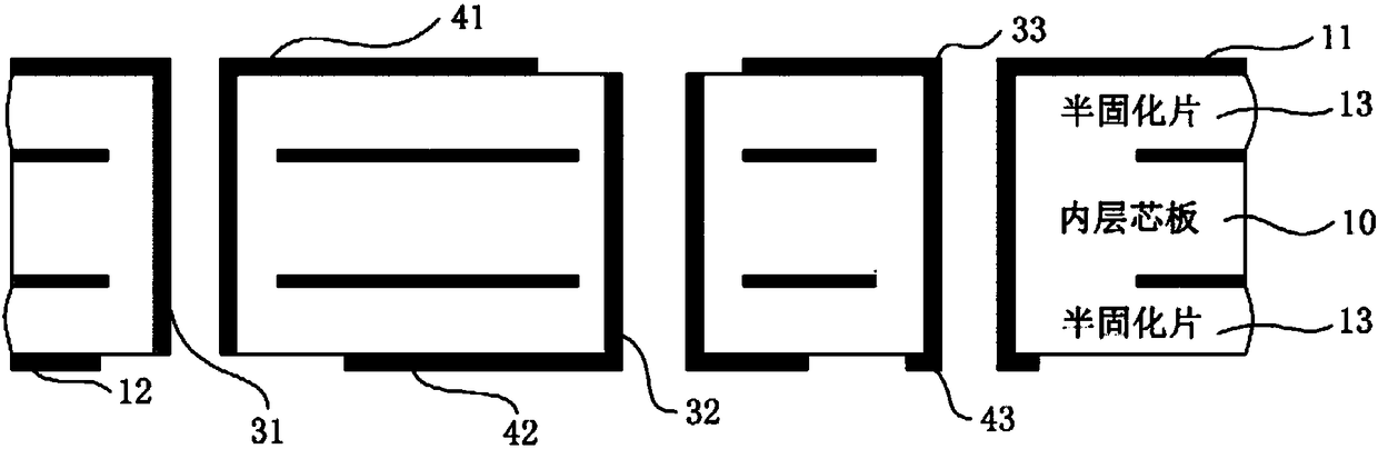
[0075] see figure 2 , the embodiment of the present invention also provides a PCB for an AC charging pile, the PCB includes an upper PCB sub-board 11 , a prepreg 13 , an inner core board 10 , a prepreg 13 and a lower PCB sub-board 12 that are sequentially stacked and pressed together. , the inner layer core board 10 is made with an inner layer circuit pattern by the first electroplating, and the outer layer circuit pattern is made on the upper layer PCB sub-board 11 and the lower layer PCB sub-board 12 through the second electroplating;

[0076] The outer layer circuit pattern is also provided with at least two copper-drawing holes that run through the PCB and avoid the inner-layer circuit pattern; one end of the copper-drawing hole is connected to the surface copper of the outer layer circuit pattern, so The other end of the drawn copper hole copper avoids the outer circuit pattern on the other side;

[0077] The pattern area of ​​the outer circuit pattern is covered with a...


PUM


Abstract

The invention provides a production method of a PCB (printed circuit board). The method comprises the steps as follows: S10, providing an inner core veneer, performing primary electroplating on the inner core veneer, and producing an inner circuit graph; S20, selecting a matched prepreg according to the adhesive flow, and laminating the inner core veneer, the prepreg, an upper sub-PCB and a lowersub-PCB to form the PCB; S30, performing drilling and secondary electroplating on the PCB to produce an outer circuit graph and at least two copper drawing holes which penetrate through the PCB and avoid the inner circuit graph; S40, baking the PCB to the preset temperature, then, spraying tin, and covering a graph zone of the outer circuit graph with an anti-corrosion tin layer. On the other hand, the invention provides the PCB applied to an alternating current charging pile. The production method of the PCB and the PCB can solve the reliability problems of copper surface warping, layering, blistering and the like, and the assembly stability of the alternating current charge pile is guaranteed.

Description

technical field [0001] The invention relates to the technical field of PCBs, in particular to a PCB manufacturing method and the PCB. Background technique [0002] With the vigorous development of the charging pile industry, it also drives the development of domestic charging pile PCBs. Compared with ordinary PCBs, PCBs used for charging piles carry larger currents and higher voltages, and PCBs used for charging piles need to withstand high voltages, and the thickness of the insulating layer should also be larger. Therefore, the conductive line of the PCB used for charging piles should be wider, and most of them are thick copper plates, which are much thicker than ordinary PCBs. If they are thin plates, they are easy to heat up and burn out, and thick copper plates can carry many and heavy electronic components after packaging. Devices, to avoid PCB deformation damage. [0003] However, due to the thick copper and board thickness of the PCB for charging piles, when the tem...

Claims


Application Information

Patent Timeline
IPC IPC(8): H05K3/46H05K1/02
CPCH05K1/0298H05K3/4611
Inventor 雷忆先严明雷胜珠
Owner SHENZHEN TONGWEIXIN CIRCUIT TECH CO LTD
Why Eureka
Try Eureka