A device and method for adjusting transistor substrate voltage and correcting on-chip non-uniformity

A technology of substrate voltage and non-uniformity, which is applied in measurement devices, radiation pyrometry, optical radiation measurement, etc., can solve the problems of low circuit expansion performance and large noise contribution, so as to improve circuit performance, reduce noise contribution, Improve the effect of application range

Active Publication Date: 2020-05-15
YANTAI RAYTRON TECH
View PDF4 Cites 0 Cited by
  • Summary
  • Abstract
  • Description
  • Claims
  • Application Information

AI Technical Summary

Problems solved by technology

[0004] The technical problem to be solved by the present invention is to provide a device and method for adjusting transistor substrate voltage and correcting on-chip non-uniformity, which is used to solve the problems of large contribution to output noise and low circuit expansion performance of on-chip non-uniform correction and adjustment voltage

Method used


Image

  • A device and method for adjusting transistor substrate voltage and correcting on-chip non-uniformity
  • A device and method for adjusting transistor substrate voltage and correcting on-chip non-uniformity
  • A device and method for adjusting transistor substrate voltage and correcting on-chip non-uniformity

Examples


Embodiment Construction

[0029] The principles and features of the present invention are described below in conjunction with the accompanying drawings, and the examples given are only used to explain the present invention, and are not intended to limit the scope of the present invention.

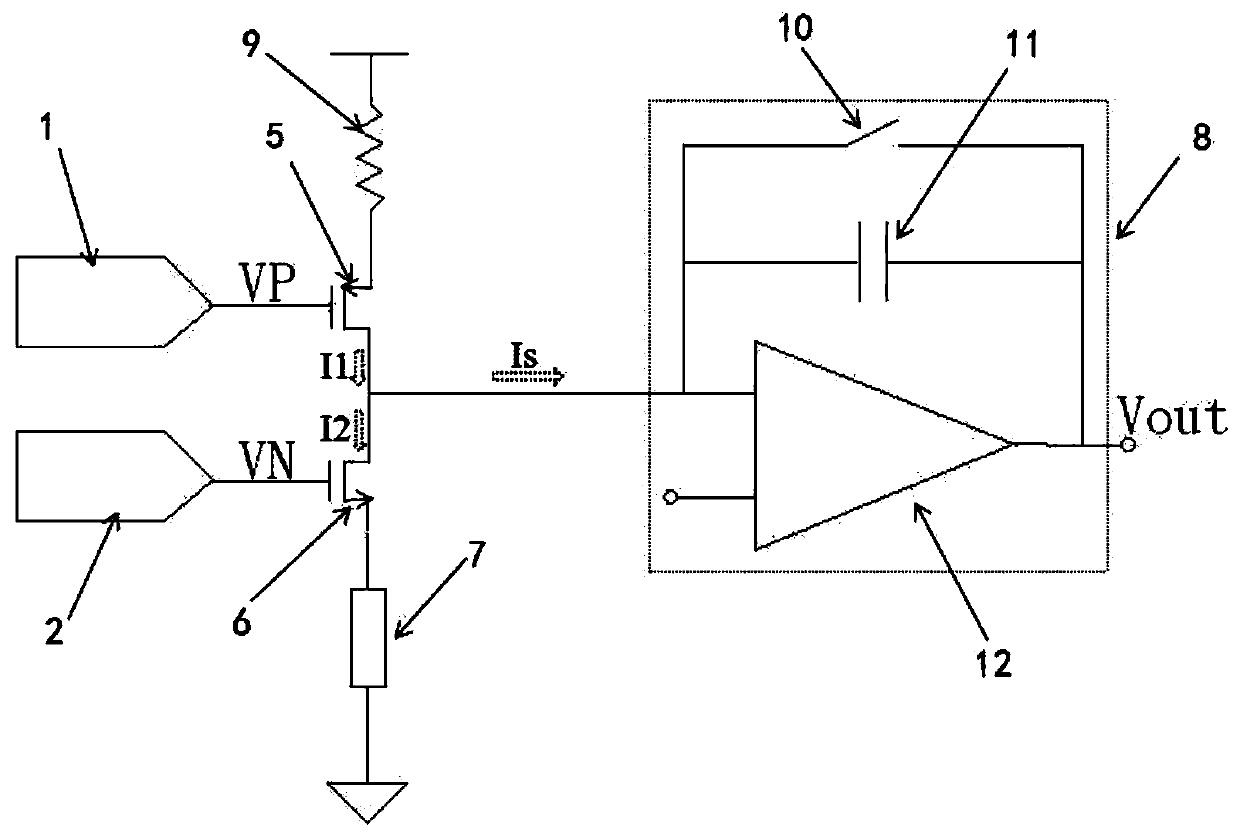
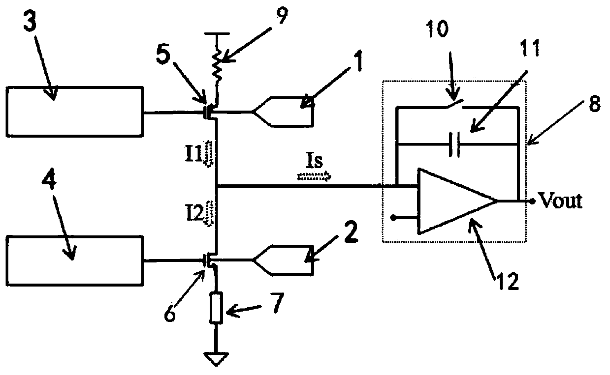
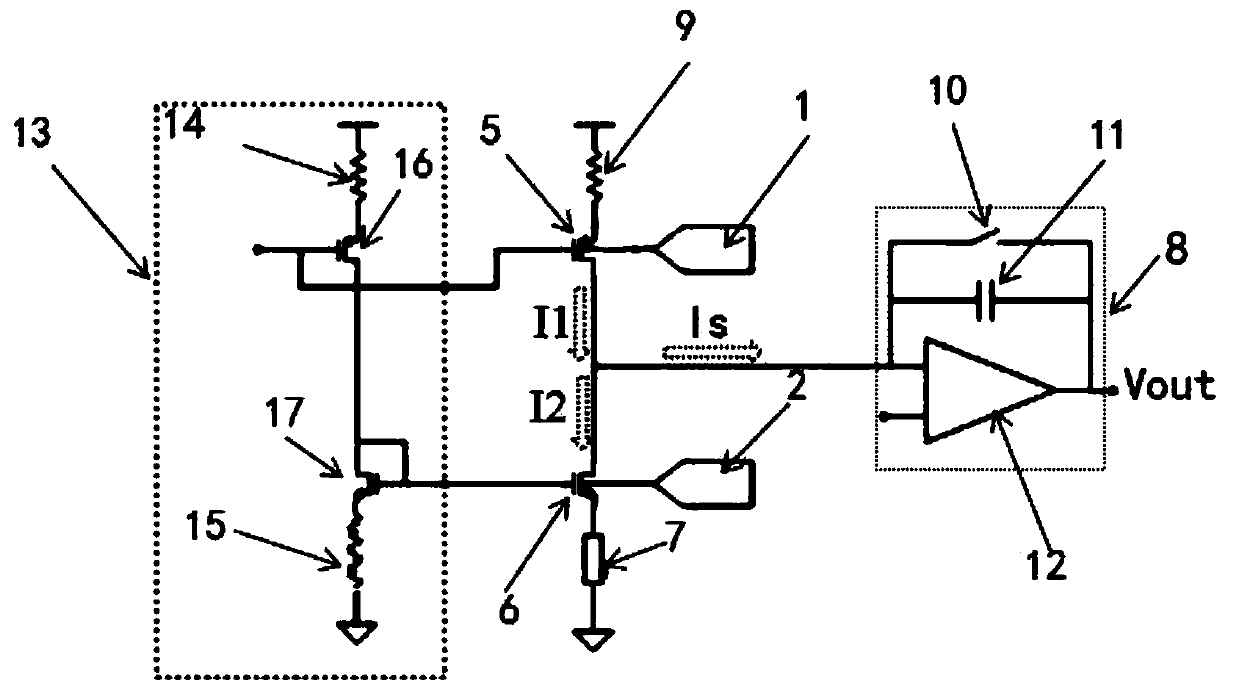
[0030] Such as figure 2 As shown, a structural schematic diagram of adjusting transistor substrate voltage to correct on-chip non-uniformity, including: a first analog-to-digital converter 1, a second analog-to-digital converter 2, a PMOS transistor 5, an NMOS transistor 6, and a sensor detection element resistance array 7. Integrating circuit 8, non-photosensitive resistor 9, functional module circuit 13, wherein, PMOS tube is a P-channel field-effect transistor, and NMOS tube is an N-channel field-effect transistor; the drain of NMOS tube 6 is connected to sensor detection element resistance array 7 , the source is respectively connected to the drain of the PMOS transistor 5 and the integration circuit 8; the sou...


PUM


Abstract

The invention relates to a device for adjusting transistor substrate voltage and correcting on-chip non-uniformity, comprising: a first analog-to-digital converter, a second analog-to-digital converter, a first functional module circuit, a second functional module circuit, a PMOS transistor, and an NMOS transistor. Tube, sensor detection element resistance array, integration circuit, non-photosensitive resistance; the drain of the NMOS tube is connected to the sensor detection element resistance array, and the source is respectively connected to the drain of the PMOS tube and the integration circuit; the source of the PMOS tube is connected to the non-photosensitive One end of the resistor is connected, and the drain is also connected to the integrating circuit; the first functional module circuit and the second functional module circuit are respectively connected to the gate of the PMOS transistor and the gate of the NMOS transistor; the first analog-to-digital converter and the second analog-to-digital converter The converter is respectively connected to the substrates of the PMOS transistor and the substrate of the NMOS transistor for adjusting the substrate voltage of the PMOS transistor and the NMOS transistor. The invention realizes the non-uniformity correction on the chip by adjusting the substrate voltage of the transistor, reduces the noise contribution of the adjusted voltage to the output during the non-uniform correction, and improves the expansion performance of the circuit.

Description

technical field [0001] The invention relates to the field of non-uniformity correction of infrared focal plane, in particular to a device and method for adjusting transistor substrate voltage to correct on-chip non-uniformity. Background technique [0002] Due to the limitations of the manufacturing process and materials, the problem of non-uniformity of the infrared focal plane array is very prominent. The existence of non-uniformity will reduce the dynamic range of the infrared detector, and the contrast of the infrared image is low. Non-uniformity exists in the form of spatially distributed noise and cannot be eliminated by averaging multiple measurements. It seriously affects the imaging quality of infrared sensors, making the acquired image signals blurred and distorted, and even makes the sensor lose its ability to detect. capacity, which must be reduced by non-uniformity correction. The non-uniformity correction technology is to correct the non-uniformity of the dete...

Claims


Application Information

Patent Timeline
Patent Type & Authority Patents(China)
IPC IPC(8): G01J5/00
CPCG01J5/00G01J5/80
Inventor 李聪科俞白军
Owner YANTAI RAYTRON TECH
Why Eureka
Try Eureka