
Inductive load-based metal-oxide semiconductor field-effect transistor (MOSFET) switch control method

An inductive load and switch control technology, applied in electronic switches, electrical components, transistors, etc., can solve problems such as unsatisfactory effects and unobvious suppression of voltage overshoot, so as to suppress oscillation and overshoot, increase damping, and reduce switching loss Effect

Inactive Publication Date: 2018-06-22
CHINA UNIV OF MINING & TECH
View PDF4 Cites 2 Cited by
  • Summary
  • Abstract
  • Description
  • Claims
  • Application Information

AI Technical Summary

Problems solved by technology

This method reduces switching loss and current overshoot to a certain extent, but the suppression of voltage overshoot is not obvious, and the effect is still not ideal

Method used


Image

  • Inductive load-based metal-oxide semiconductor field-effect transistor (MOSFET) switch control method
  • Inductive load-based metal-oxide semiconductor field-effect transistor (MOSFET) switch control method
  • Inductive load-based metal-oxide semiconductor field-effect transistor (MOSFET) switch control method

Examples


Embodiment Construction

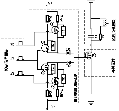
[0025] The following is attached figure 1 , the specific implementation manner of the present invention will be further described in detail, so as to make the method easier to understand and master.

[0026] The method for controlling a switching device under an inductive load includes: a control signal module, a grid resistance switching module, a load module and a switching device; it is characterized in that the control signal module is connected to the grid resistance switching module, The gate resistance switching module is connected to the external power supply and the gate of the switching device, the drain of the switching device is connected to the positive pole of the power supply in series with the inductive load module, and the source of the switching device is connected to the negative pole of the power supply.

[0027] The control signal module outputs a control signal to control the MOSFET in the gate resistance switching module to turn on and off at an appropr...


PUM


Abstract

The invention relates to an inductive load-based metal-oxide semiconductor field-effect transistor (MOSFET) switch control method, solving problems of loss and off peak in on and off of the MOSFET device under inductive load. The method uses a control signal module, a gate resistance switch module, an inductive load module and a switch device. The method is characterized in that the control signalmodule outputs a control signal to the gate resistance switch module, based on different control signals, the gate resistance switch module uses a proper gate resistance group to control on and off of the switch device, finally, the on and off loss is lowered, and voltage and current oscillation and overshoot are prohibited.

Description

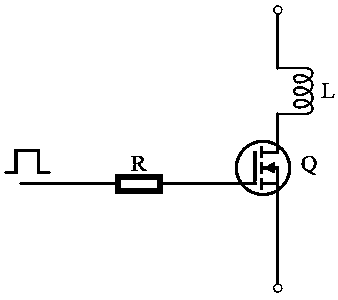
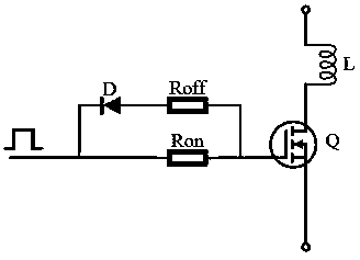
technical field [0001] The invention relates to a method for controlling a switching device, in particular to a method for controlling a MOSFET switch under an inductive load. Background technique [0002] In recent years, with the continuous development of power electronics technology, power semiconductor switching device MOSFET has been applied in more and more occasions. Since there are a large number of inductive loads in the industrial field, such as AC and DC relays, contactors, transformers, and AC and DC electromagnets, when switching operations are performed on them, extremely high voltage and current will be generated at both ends of the inductance coil. Oscillation and overshoot threaten the safe operation of the system. In addition, the switching losses of power semiconductor switching devices also account for a large proportion of the total losses. [0003] Therefore, as the requirements for switching frequency become higher and higher, the optimization of swi...

Claims


Application Information

Patent Timeline
IPC IPC(8): H03K17/695H03K17/081H03K17/14H03K17/041
CPCH03K17/04106H03K17/08104H03K17/145H03K17/687
Inventor 蔺志佳刘任豪张雪
Owner CHINA UNIV OF MINING & TECH
Learn More