Method for preparing HfS2/h-BN heterojunction material by selective patterning

A hafnium disulfide, selective technology, applied in semiconductor/solid-state device manufacturing, electrical components, circuits, etc., can solve the problems of small sample size, strong randomness in the preparation process, uncontrollable material thickness, etc., to achieve simple preparation process, The effect of low production cost

Inactive Publication Date: 2018-06-22
INST OF SEMICONDUCTORS - CHINESE ACAD OF SCI
View PDF6 Cites 4 Cited by
  • Summary
  • Abstract
  • Description
  • Claims
  • Application Information

AI Technical Summary

Problems solved by technology

[0005] But currently about HfS 2 There are still many problems to be solved in the research of / h-BN heterojunction materials
Especially in the lack of exploration on material growth, HfS prepared by mechanical exfoliation 2 / h-BN heterojunction materials have problems such as small sample size, uncontrollable material thickness, and strong randomness in the preparation process, which largely limits its large-scale integrated production

Method used


Image

  • Method for preparing HfS2/h-BN heterojunction material by selective patterning
  • Method for preparing HfS2/h-BN heterojunction material by selective patterning
  • Method for preparing HfS2/h-BN heterojunction material by selective patterning

Examples


Embodiment Construction

[0017] In order to make the object, technical solution and advantages of the present invention clearer, the present invention will be described in further detail below in conjunction with specific embodiments and with reference to the accompanying drawings.

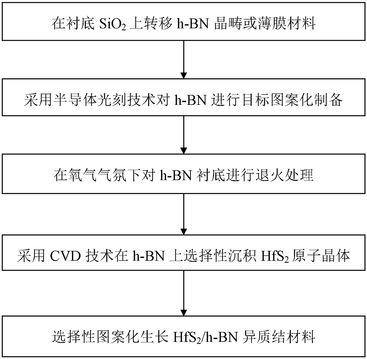
[0018] In an exemplary embodiment of the present invention, a selective patterning method for preparing hafnium disulfide boron nitride HfS 2 / h-BN heterojunction material method, which includes the following steps: step 1, h-BN crystal domain or thin film material is transferred to the target substrate SiO 2 On; step 2, transferring to the target substrate SiO 2 The h-BN on the target patterning photolithography; step 3, annealing the h-BN substrate in an oxygen atmosphere to remove the residual organic matter on the h-BN surface; step 4, after the annealing is completed, the h-BN Growth of HfS on the substrate surface 2 Atomic crystals, selective preparation of HfS 2 / h-BN heterojunction material.

[0019] Specifica...


PUM


Abstract

The invention provides a method for preparing an HfS2/h-BN heterojunction material by selective patterning. The method comprises the following steps of 1, transferring an h-BN crystal domain or a thinfilm material to a target substrate; 2, performing target patterning photoetching on h-BN transferred onto the target substrate; 3, annealing the h-BN substrate under an oxygen atmosphere to remove an organic matter resided on a surface of the h-BN; and 4, growing an HfS2 atomic crystal on a surface of the h-BN substrate after annealing is completed, and selectively preparing the HfS2/h-BN heterojunction material. The HfS2/h-BN heterojunction material is simple in preparation process, low in cost and high in controllability, and importance significance is brought to mass integrated productionand application of an HfS2/h-BN material-based photoelectric device.

Description

technical field [0001] The invention relates to the technical field of nanomaterial preparation, in particular to a method for selectively patterning and preparing hafnium disulfide boron nitride heterojunction materials. Background technique [0002] In recent years, in electronics and optoelectronics, due to the zero bandgap characteristics of graphene, its poor light absorption ability and low switching ratio limit its further application. Therefore, people have turned their research focus to transition metal chalcogenides (TMDs, MX 2 , M is a transition metal such as Mo, Hf, etc., X is S, Se, etc.). The material has many excellent physical properties. First, TMDs have a natural band gap that graphene materials lack. Furthermore, TMDs have a photoluminescence phenomenon, which provides unlimited possibilities for their application in optoelectronic devices. In addition, TMDs have good flexibility and transparency, and single-layer TMDs field-effect transistors have gr...

Claims


Application Information

Patent Timeline
Patent Type & Authority Applications(China)
IPC IPC(8): H01L21/18H01L21/027H01L21/324
Inventor 王登贵张兴旺尹志岗孟军华
Owner INST OF SEMICONDUCTORS - CHINESE ACAD OF SCI
Why Eureka
Try Eureka