Image sensor and method for forming same

An image sensor and side edge technology, applied in the direction of electric solid-state devices, semiconductor devices, electrical components, etc., can solve the problems that the performance of CMOS image sensors needs to be improved, and achieve the expansion of the photosensitive dynamic range, the reduction of the probability of recombination, and the average path length Reduced effect

Inactive Publication Date: 2018-06-19
HUAIAN IMAGING DEVICE MFGR CORP
View PDF5 Cites 1 Cited by
  • Summary
  • Abstract
  • Description
  • Claims
  • Application Information

AI Technical Summary

Problems solved by technology

[0004] However, the performance of existing CMOS image sensors needs to be improved

Method used


Image

  • Image sensor and method for forming same
  • Image sensor and method for forming same
  • Image sensor and method for forming same

Examples


Embodiment Construction

[0022] As mentioned in the background, the performance of the image sensor formed by the prior art is relatively poor.

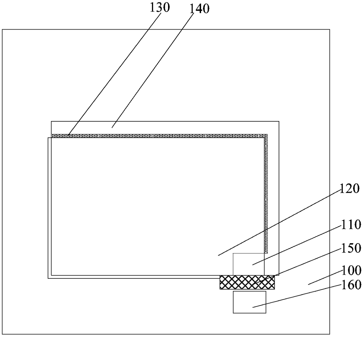
[0023] An image sensor, reference figure 1 , including: a substrate 100, the substrate 100 including a diode region and a capacitor region adjacent to the diode region, the diode region has opposite first side edges and second side edges, and opposite third side edges and fourth sides edge, the capacitance region is adjacent to only the first side edge and the third side edge of the diode region; the diode region includes a diode body region and a charge storage region, and the charge storage region is located in the diode region by the second side edge and the third The corner where the side edges intersect; the photodiode 120 located in the diode body region; the capacitor dielectric layer 130 and the capacitor gate 140 located in the capacitor body region, and the capacitor dielectric layer 130 is located between the capacitor gate 140 and the photodiode ...


PUM


Abstract

An image sensor and a method for forming the same are provided. The image sensor comprises: a diode region including a diode body region and a first charge storage region, wherein the first charge storage region is located at a corner formed by intersecting a first side edge with a third side edge intersect in the diode region; a capacitor region including a capacitor body region adjacent to the diode body region and a second charge storage region adjacent to the first charge storage region, wherein the second charge storage region and the capacitor body region are adjacent to each other; a photodiode located in the diode body region; a capacitor dielectric layer and a capacitor gate located in the capacitor body region, wherein the capacitor dielectric layer is located between the capacitor gate and the photodiode; and a charge storage layer located in the first charge storage region and the second charge storage region, wherein the charge storage layer is connected with the capacitorgate. The performance of the image sensor is improved.

Description

technical field [0001] The invention relates to the field of semiconductor manufacturing, in particular to an image sensor and a forming method thereof. Background technique [0002] An image sensor is a semiconductor device that converts light signals into electrical signals. [0003] Image sensors are classified into complementary metal oxide (CMOS) image sensors and charge coupled device (CCD) image sensors. CMOS image sensor has the advantages of simple process, easy integration of other devices, small size, light weight, low power consumption and low cost. Therefore, with the development of image sensing technology, CMOS image sensors are increasingly used in various electronic products instead of CCD image sensors. At present, CMOS image sensors have been widely used in still digital cameras, digital video cameras, medical imaging devices, and automotive imaging devices. [0004] However, the performance of existing CMOS image sensors needs to be improved. Content...

Claims


Application Information

Patent Timeline
Patent Type & Authority Applications(China)
IPC IPC(8): H01L27/146
CPCH01L27/14601H01L27/14643H01L27/14683
Inventor 穆钰平柯天琪黄晓橹
Owner HUAIAN IMAGING DEVICE MFGR CORP
Why Eureka
Try Eureka