Film bulk acoustic wave resonator
A thin-film bulk acoustic wave and resonator technology, applied to electrical components, impedance networks, etc., can solve the problems of strengthening standing wave reflection energy and reducing Q value, and achieve the effect of reducing reflection energy and improving Q value
- Summary
- Abstract
- Description
- Claims
- Application Information
AI Technical Summary
Problems solved by technology
Method used
Image

Examples
Embodiment 1
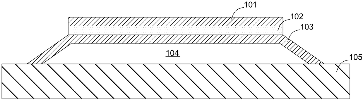
[0032] This embodiment provides a thin film bulk acoustic resonator, such as Figure 4 As shown, it includes a substrate 105, a bottom electrode 103, a piezoelectric layer 102, and a top electrode 101 arranged sequentially from bottom to top, wherein a reflective interface is provided between the substrate 105 and the bottom electrode 103, and the bottom electrode 103, the piezoelectric layer At least one of the electrical layer 102 and the top electrode 101 is added with at least one bump of the same material as the original structure of the layer; the thickness of the bump is consistent with the original structure of the layer. Then, the manufacturing process of the bump is the same as that of other structures in the layer, and only one more bump needs to be grown during the manufacturing.
[0033] In this embodiment, the bump is an independent bump with a certain distance (greater than 0, less than or equal to 100 um) from the original structure of the layer. To further il...
Embodiment 2
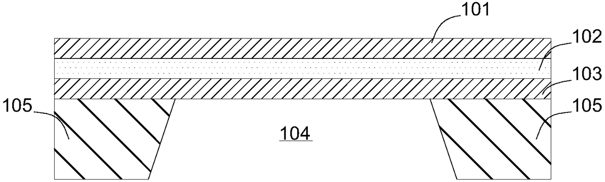
[0038] The structure and principle of this embodiment are the same as Embodiment 1, the difference is: Figure 5 As shown, the bump is a connecting bump connected to the original structure of the layer. The thickness of the connection bump is consistent with the layer it is on. The preparation process of the connecting bump is the same as that of other structures in the layer, and only the shape of the outer contour needs to be controlled during the preparation.
[0039] The longest dimension of the connection bump is 1nm-100um.
[0040] Taking the top electrode 101 as an example, three connection bumps 1014 are connected at any position on the outer contour 1011 of the top electrode. In addition, one connection bump 1014 may be connected to the top electrode 101 , two connection bumps may be connected to the piezoelectric layer 102 , and three connection bumps may be connected to the bottom electrode 103 . The number of connection bumps in each layer is not limited, and th...
Embodiment 3
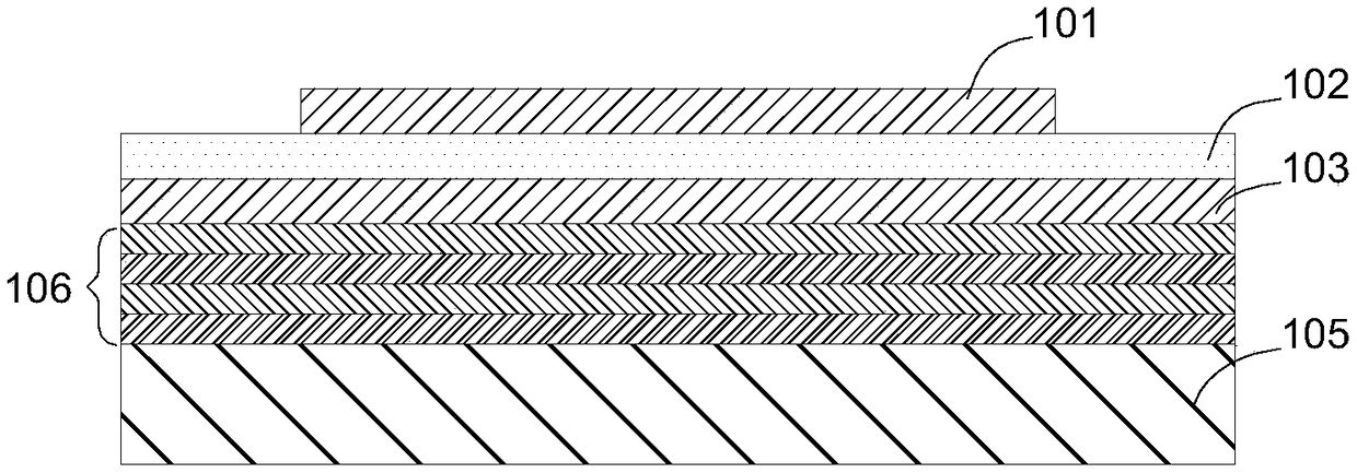
[0044] This embodiment provides a thin film bulk acoustic resonator, comprising a substrate 105, a bottom electrode 103, a piezoelectric layer 102 and a top electrode 101 arranged in sequence from bottom to top, wherein a reflective interface is provided between the substrate 105 and the bottom electrode 103, At least one of the bottom electrode 103 , the piezoelectric layer 102 and the top electrode 101 is provided with a missing block, and the missing block is located in the original structure and is close to the edge of the active area. The clear definition of the active area is: the overlapping area of the top electrode 101 , the piezoelectric layer 102 and the bottom electrode 103 , and there is a reflective interface under the overlapping area.
[0045] Taking the top electrode 101 as an example, as Figure 6 As shown, there is at least one missing piece 1015 at any position in the middle of the top electrode 101 . The height of the missing piece 1015 is less than or ...
PUM
| Property | Measurement | Unit |
|---|---|---|
| Longest size | aaaaa | aaaaa |
Abstract
Description
Claims
Application Information
 - Generate Ideas
- Intellectual Property
- Life Sciences
- Materials
- Tech Scout
- Unparalleled Data Quality
- Higher Quality Content
- 60% Fewer Hallucinations
Browse by: Latest US Patents, China's latest patents, Technical Efficacy Thesaurus, Application Domain, Technology Topic, Popular Technical Reports.
© 2025 PatSnap. All rights reserved.Legal|Privacy policy|Modern Slavery Act Transparency Statement|Sitemap|About US| Contact US: help@patsnap.com