Nano porous surface plasmon crystal and preparation method thereof
A surface plasmon and nanoporous technology, applied in crystal growth, nanotechnology, polycrystalline material growth, etc., can solve the problems of poor optical properties of surface plasmon crystals, achieve excellent optical characteristics, and obviously economical Benefits, industrial simplicity of preparation
- Summary
- Abstract
- Description
- Claims
- Application Information
AI Technical Summary
Problems solved by technology
Method used
Image
Examples
preparation example Construction
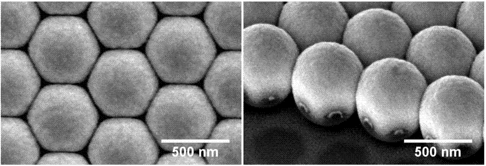
[0036] The invention provides a method for preparing a nanoporous surface plasmon crystal, comprising the following steps:
[0037] a. The nano-microsphere suspension is formed into single dispersed nano-microspheres on the surface of the silicon wafer by a spin-coating method;
[0038] b. Assembling the single dispersed nanospheres obtained in step a onto the surface of the substrate by using a gas / liquid interface self-assembly method to form a regular two-dimensional hexagonal close-packed nanosphere array;
[0039] c. annealing the two-dimensional hexagonal close-packed nanosphere array obtained in step b;
[0040] d. Depositing an alloy thin film on the surface of the two-dimensional hexagonal close-packed nano-microsphere array after the annealing in step c by using a physical vapor deposition method to form an array of metal alloy hemispherical shells;
[0041] e. Dealloying the array obtained in step d in an electrolyte solution to form a nanoporous metal hemispherica...
Embodiment 1
[0061] Example 1 Using the method of the present invention to prepare nanoporous surface plasmon crystals
[0062] (1) Place the silicon wafer with a diameter of 2 inches after hydrophilic treatment in a spin coater, and use a pipette to drop 100 μl of polystyrene microsphere suspension with a diameter of 500 nm and a concentration of 2.5 wt% onto the silicon wafer , set the spin-coating program as follows: the first step is 600rpm for 20s, and the second step is 2500rpm for 40s. Start the spin coater for spin coating. The samples were removed after spin coating.
[0063] (2) Add a sufficient amount of deionized water to a petri dish with a diameter of 15 cm, add 5 μl of sodium dodecyl sulfate dropwise in the deionized water, and then place the sample in step 1 incline slowly in deionized water to make the surface of the poly Styrene microspheres self-assembled on the water surface to form a dense and regularly arranged monolayer array. The single-layer polystyrene array on...
Embodiment 2
[0067] Example 2 Using the method of the present invention to prepare nanoporous surface plasmon crystals
[0068] (1) Place the silicon wafer with a diameter of 2 inches after hydrophilic treatment in a spin coater, and use a pipette to drop 100 μl of polystyrene microsphere suspension with a diameter of 500 nm and a concentration of 2.5 wt% onto the silicon wafer , set the spin-coating program as follows: the first step is 600rpm for 20s, and the second step is 2500rpm for 40s. Start the spin coater for spin coating. The samples were removed after spin coating.
[0069] (2) Add a sufficient amount of deionized water to a petri dish with a diameter of 15 cm, add 5 μl of sodium dodecyl sulfate dropwise in the deionized water, and then place the sample in step 1 incline slowly in deionized water to make the surface of the poly Styrene microspheres self-assembled on the water surface to form a dense and regularly arranged monolayer array. The single-layer polystyrene array on...
PUM
| Property | Measurement | Unit |
|---|---|---|
| diameter | aaaaa | aaaaa |
| diameter | aaaaa | aaaaa |
| diameter | aaaaa | aaaaa |
Abstract
Description
Claims
Application Information
 - R&D
- Intellectual Property
- Life Sciences
- Materials
- Tech Scout
- Unparalleled Data Quality
- Higher Quality Content
- 60% Fewer Hallucinations
Browse by: Latest US Patents, China's latest patents, Technical Efficacy Thesaurus, Application Domain, Technology Topic, Popular Technical Reports.
© 2025 PatSnap. All rights reserved.Legal|Privacy policy|Modern Slavery Act Transparency Statement|Sitemap|About US| Contact US: help@patsnap.com


