Preparation method of Ag nanoparticle loaded ZnO film
A nanoparticle and thin film technology is applied in the field of preparation of Ag nanoparticle-supported ZnO thin films, which can solve the problems of unsatisfactory electrochemical performance, expensive chemical reagents, complicated preparation process, etc., and achieve improved electrochemical performance, low price, and preparation process. simple effect
- Summary
- Abstract
- Description
- Claims
- Application Information
AI Technical Summary
Problems solved by technology
Method used
Image
Examples
Embodiment 1
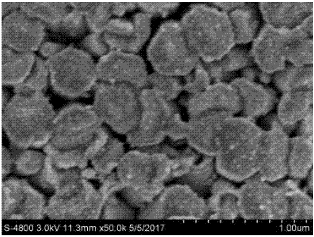
[0041] The invention discloses a method for preparing a ZnO thin film supported by Ag nanoparticles, comprising preparing the ZnO thin film, uniformly mixing the prepared ZnO thin film with a silver nitrate solution, and obtaining the ZnO thin film supported by Ag nano particles after being irradiated with ultraviolet light.
Embodiment 2
[0043] A preparation method of Ag nanoparticles loaded ZnO film, comprising the steps of:
[0044] S1. Preparation of ZnO seed layer: After ultrasonically cleaning a single-polished silicon wafer with a size of 15mm×15mm×1mm in acetone and deionized water for 20 minutes, place it in an oven at 60°C, and dry it in the atmosphere to obtain a spare silicon wafer. slices; mix the zinc acetate solution and stabilizer evenly, put it in a magnetic stirring water bath, heat up, keep warm, cool down, and stand still to obtain the ZnO precursor solution; use the film throwing method to coat the ZnO precursor solution on the spare silicon wafer Finally, successively carry out glue dropping, glue homogenization, primary pretreatment, cooling to room temperature, secondary pretreatment, and annealing in a high-temperature tube furnace to obtain a ZnO seed layer;
[0045] S2. Preparation of ZnO film: Pour the solution containing zinc ions prepared by dissolving zinc nitrate hexahydrate and ...
Embodiment 3
[0063] A preparation method of Ag nanoparticles loaded ZnO film, comprising the steps of:
[0064] S1. Preparation of ZnO seed layer: After ultrasonically cleaning a single-polished silicon wafer with a size of 15mm×15mm×1mm in acetone and deionized water for 20 minutes, place it in an oven at 60°C, and dry it in the atmosphere to obtain a spare silicon wafer. slices; mix the zinc acetate solution and stabilizer evenly, put it in a magnetic stirring water bath, heat up, keep warm, cool down, and stand still to obtain the ZnO precursor solution; use the film throwing method to coat the ZnO precursor solution on the spare silicon wafer Finally, successively carry out glue dropping, glue homogenization, primary pretreatment, cooling to room temperature, secondary pretreatment, and annealing in a high-temperature tube furnace to obtain a ZnO seed layer;
[0065] S2. Preparation of ZnO film: Pour the solution containing zinc ions prepared by dissolving zinc nitrate hexahydrate and ...
PUM
| Property | Measurement | Unit |
|---|---|---|
| wavelength | aaaaa | aaaaa |
| wavelength | aaaaa | aaaaa |
| wavelength | aaaaa | aaaaa |
Abstract
Description
Claims
Application Information
 - R&D
- Intellectual Property
- Life Sciences
- Materials
- Tech Scout
- Unparalleled Data Quality
- Higher Quality Content
- 60% Fewer Hallucinations
Browse by: Latest US Patents, China's latest patents, Technical Efficacy Thesaurus, Application Domain, Technology Topic, Popular Technical Reports.
© 2025 PatSnap. All rights reserved.Legal|Privacy policy|Modern Slavery Act Transparency Statement|Sitemap|About US| Contact US: help@patsnap.com


