Piezoelectric-electromagnetic hybrid vibration energy collector and preparation method thereof
A technology of vibration energy collection and electromagnetic compounding, which is applied in the direction of piezoelectric effect/electrostrictive or magnetostrictive motors, generators/motors, electrical components, etc., can solve the problems of low energy collection efficiency, single vibration pickup structure, output Low current and other problems, to achieve the effect of compact structure, small size and high output power density
- Summary
- Abstract
- Description
- Claims
- Application Information
AI Technical Summary
Problems solved by technology
Method used
Image
Examples
Embodiment 1
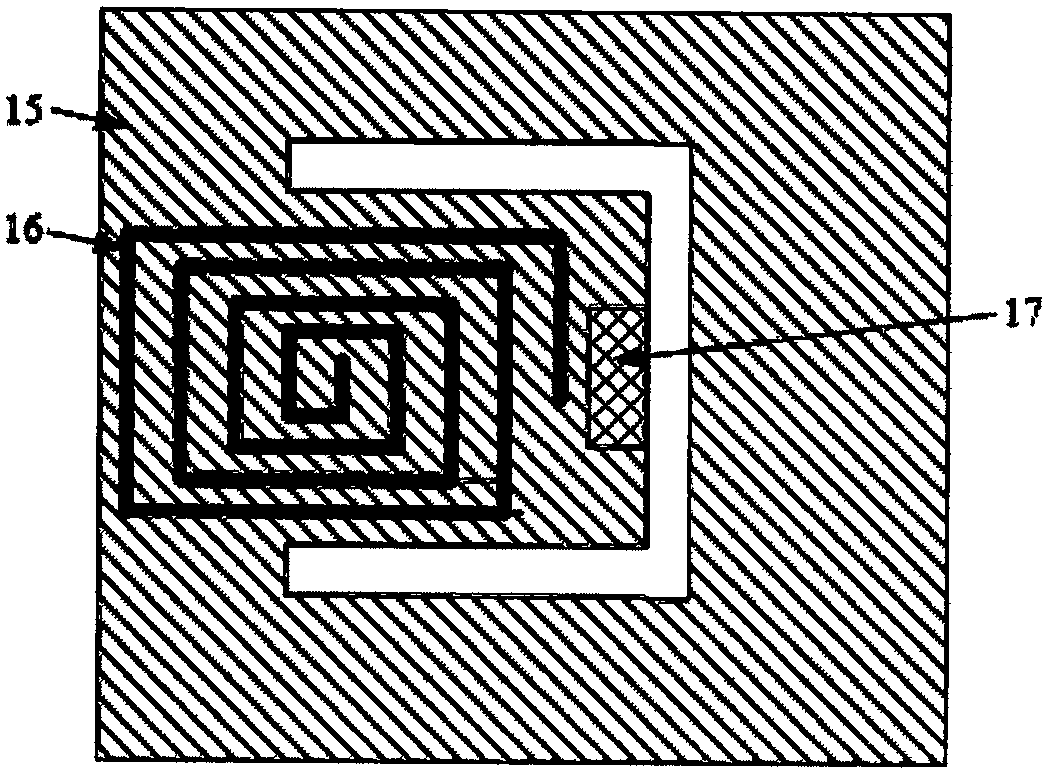
[0034] see figure 1 and figure 2 , the present invention provides a piezoelectric-electromagnetic composite vibration energy harvester, the piezoelectric-electromagnetic composite vibration energy harvester has multiple vibration pickup structures and resonance frequencies, and can obtain high energy collection efficiency.
[0035] The piezoelectric-electromagnetic composite vibration energy harvester includes: a first substrate 10, a second substrate 20 and a third substrate 30 stacked on each other; the first substrate 10 and the third substrate 30 are respectively formed by etching The first and second cantilever beam structures, wherein a first groove 19 is formed on the lower surface of the first substrate 10, a first cantilever beam structure is formed above the first groove 19, and a first cantilever beam structure is formed on the upper surface of the third substrate 30. Below the second groove 39 and the second groove 39 is a second cantilever beam structure.
[00...
Embodiment 2
[0054] The present invention also provides a preparation method of a piezoelectric-electromagnetic composite vibration energy harvester, the preparation method comprising the following steps:
[0055] A first substrate is selected, and the lower surface of the first substrate is etched to form a first groove structure. For example, N(100) silicon with a thickness of 500 μm is selected as the first substrate, and Si with a thickness of 200 nm is grown on the lower surface of the substrate by, for example, a low-pressure chemical vapor deposition method. 3 N 4 ; Etching the Si on the lower surface of the first substrate 3 N 4 , with Si 3 N 4 Use TMAH (tetramethylammonium hydroxide) reagent as a mask to perform wet etching on the silicon substrate to form a first groove as deep as 450 μm.
[0056] A first inductive coil layer is formed by depositing and etching on the first piezoelectric layer. Specifically, when using H 3 PO 4 solution to remove Si from silicon wafer sur...
PUM
 Abstract
Description
Claims
Application Information
 - R&D
- Intellectual Property
- Life Sciences
- Materials
- Tech Scout
- Unparalleled Data Quality
- Higher Quality Content
- 60% Fewer Hallucinations
Browse by: Latest US Patents, China's latest patents, Technical Efficacy Thesaurus, Application Domain, Technology Topic, Popular Technical Reports.
© 2025 PatSnap. All rights reserved.Legal|Privacy policy|Modern Slavery Act Transparency Statement|Sitemap|About US| Contact US: help@patsnap.com


