Diamond substrate and method for producing diamond substrate

A diamond and substrate technology, applied in chemical instruments and methods, semiconductor/solid-state device manufacturing, crystal growth, etc., can solve problems such as inability to manufacture diamond substrates

Inactive Publication Date: 2018-04-17
NAMIKI PRECISION JEWEL CO LTD
View PDF5 Cites 0 Cited by
  • Summary
  • Abstract
  • Description
  • Claims
  • Application Information

AI Technical Summary

Problems solved by technology

However, for the existing HTHP method, it is impossible to manufacture large-area diamond substrates

Method used


Image

  • Diamond substrate and method for producing diamond substrate
  • Diamond substrate and method for producing diamond substrate
  • Diamond substrate and method for producing diamond substrate

Examples


Embodiment Construction

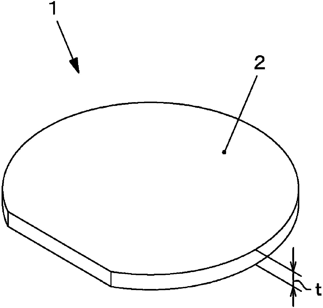
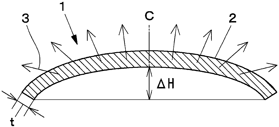
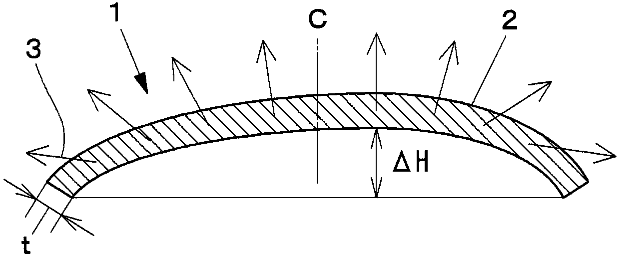
[0057] The first feature of this embodiment is that the diamond substrate is composed of a diamond single crystal, the difference between the highest part and the lowest part in the thickness direction of the diamond substrate exceeds 0 μm and is 485 μm or less, and the deviation of the crystal axis angle over the entire surface of the diamond substrate is More than 0° and less than 3.00°. According to this structure, the crystal axis of the semiconductor film formed on the entire surface of the diamond substrate can be reduced from the influence of the deviation of the crystal axis of the diamond substrate, so the angle deviation of the crystal axis of the semiconductor film is reduced, and the deviation of the semiconductor film can be suppressed. Properties deviate within the plane. At the same time, when heating a functional thin film (such as a semiconductor film, etc.) during film formation, the temperature in the surface of the diamond substrate can be made more uniform...


PUM

PropertyMeasurementUnit
surface roughnessaaaaaaaaaa
lengthaaaaaaaaaa

Abstract

To provide: a substrate comprising diamond which is free-standing, in which warpage is suppressed, and variation in the angles of the crystal axis over the entire surface of the substrate is suppressed; and a method for producing the diamond substrate. In the present invention, an underlying substrate is prepared and multiple columnar diamonds comprising diamond single crystals are formed on one side of the underlying substrate. The diamond single crystals are grown from the tip of each columnar diamond and the diamond single crystals grown from the tip of each columnar diamond are coalesced to form a diamond substrate layer which is separated from the underlying substrate to produce a diamond substrate from the diamond substrate layer. Thus, the difference between the highest portion andthe lowest portion of the diamond substrate in the thickness direction is over 0 um and 485 um or less, and the variation in the angles of the crystal axis over the entire surface of the diamond substrate is over 0 and 3.00-degree or less.

Description

technical field [0001] The present invention relates to a diamond substrate and a method for manufacturing the diamond substrate. Background technique [0002] As a semiconductor material, diamond has many incomparable excellent properties, and it is expected to be the ultimate semiconductor substrate. In particular, in recent years, diamond thin-film devices such as ultraviolet light-emitting elements exhibiting a wide bandgap and field-effect transistors having excellent high-frequency characteristics have been continuously developed. [0003] The above-mentioned diamond thin film device is made by plasma CVD (Chemical Vapor Deposition: Chemical Vapor Deposition) method. In this case, metal or silicon can be used as the base substrate for growing the diamond thin film. In order to obtain a diamond thin film with higher crystallinity, it is preferable to homoepitaxially grow the diamond thin film by using a diamond substrate as the base substrate, so that the characterist...

Claims


Application Information

Patent Timeline
Patent Type & Authority Applications(China)
IPC IPC(8): C30B29/04
CPCC30B29/04C30B25/186H01L21/02024H01L21/02527H01L21/0262H01L21/30625H01L29/0657H01L29/1602
Inventor 会田英雄小山浩司池尻宪次朗金圣祐菊地祐贵
Owner NAMIKI PRECISION JEWEL CO LTD
Why Eureka
Try Eureka