
Photomask structure and method for forming through holes in negative photoresistive pattern, as well as application

A technology of negative photoresist and via hole, which is applied in the field of photomask structure, can solve the problems of upper protective layer film rupture, reduce pixel aperture ratio, and affect display effect, so as to improve product quality and yield, improve electrical connection quality, The effect of increasing exposure

Inactive Publication Date: 2018-04-13
TCL CHINA STAR OPTOELECTRONICS TECH CO LTD
View PDF5 Cites 4 Cited by
  • Summary
  • Abstract
  • Description
  • Claims
  • Application Information

AI Technical Summary

Problems solved by technology

[0004] COA products need to form via holes on the color resistance pattern by weak exposure, but when the color resistance is weakly exposed, the crosslinking reaction of the color resistance material is not complete, the material property is unstable, the product reliability is poor, and abnormal bubbles are easy to form
If the exposure capability is increased, the slope at the position of the color-resist via hole will be too steep, resulting in the rupture of the upper protective layer, and also causing bubbles or afterimage problems.
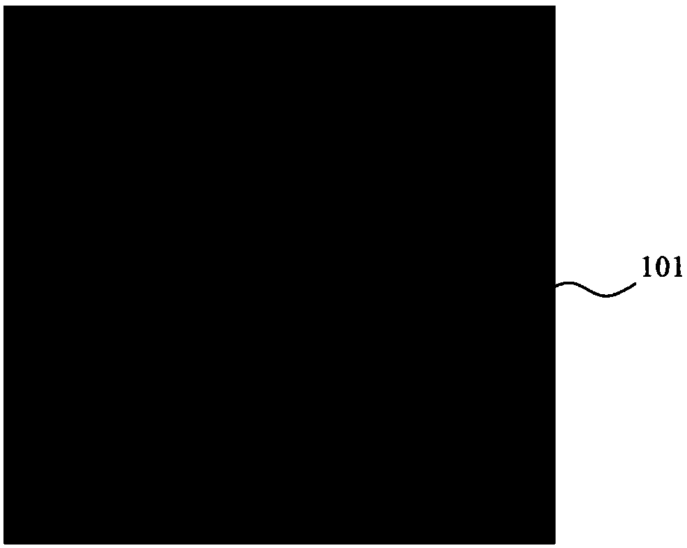
[0005] combine figure 1 and figure 2 As shown, in a prior art, a plurality of light-shielding parts 101 are provided on the mask, and each light-shielding part 101 is respectively corresponding to the upper part of the via hole 201 to be formed in the color-resist pattern. The surface of the light-shielding parts 101 is continuous and completely opaque. , the existing problems at least include: the thickness and slope (Taper) of the color filter layer at the via hole are not easy to control, and the slope is steep, which is likely to cause the pixel electrode in the via hole to break, resulting in a gap between the pixel electrode and the metal signal line. The electrical connection between them is not good, resulting in poor display of the product
To ensure a good electrical connection, it is necessary to make via holes with larger sizes, which will undoubtedly reduce the pixel aperture ratio, and the situation that the via holes are too large will easily cause the gas to leak out due to vibration after the box alignment process and spread. To the liquid crystal layer, resulting in bubbles (Bubble) and the formation of black clusters, affecting the display effect

Method used


Image

  • Photomask structure and method for forming through holes in negative photoresistive pattern, as well as application
  • Photomask structure and method for forming through holes in negative photoresistive pattern, as well as application
  • Photomask structure and method for forming through holes in negative photoresistive pattern, as well as application

Examples


Embodiment Construction

[0036] The technical solutions of the present invention will be clearly and completely described below in conjunction with the accompanying drawings. Apparently, the described embodiments are some of the embodiments of the present invention, but not all of them. Based on the embodiments of the present invention, all other embodiments obtained by persons of ordinary skill in the art without making creative efforts belong to the protection scope of the present invention.

[0037] In the description of the present invention, it should be noted that the terms "center", "upper", "lower", "left", "right", "vertical", "horizontal", "inner", "outer" etc. The indicated orientation or positional relationship is based on the orientation or positional relationship shown in the drawings, and is only for the convenience of describing the present invention and simplifying the description, rather than indicating or implying that the referred device or element must have a specific orientation, ...


PUM


Abstract

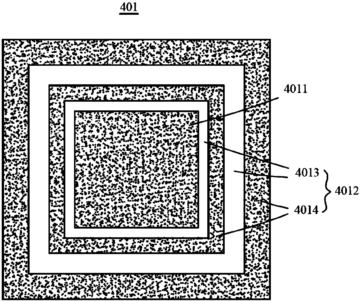
The application discloses a photomask structure and a method for forming through holes in a negative photoresistive pattern, as well as application. The photoresistive structure comprises shading parts corresponding to the through holes, each shading part is defined with a central shading region and a peripheral shading region distributed around the central shading region, a plurality of vertically hollowed slits are distributed in an array in the peripheral shading regions in at least one radial direction of the shading parts, and the widths of the slits meet: bn is larger than bn+1, where bnand bn+1 are the widths of two adjacent slits and bn is farther away from the central shading region compared with the slit corresponding to bn+1. According to the photomask structure, the method andthe application, the hollowed slits are formed in the array in the shading parts, so that the exposure of the positions of the through holes is increased; gentle slopes are formed on the edges of thethrough holes, so that the quality of electrical connections between pixel electrodes and signal wires of metal layers of thin film transistors is improved, meanwhile, film breakage of protective layers in a back-end process is reduced, and the quality and the yield of a product is improved.

Description

technical field [0001] The present application relates to the technical field of liquid crystal display device manufacturing process, in particular to a photomask structure, method and application for forming via holes on a negative photoresist pattern. Background technique [0002] At present, in order to increase the aperture ratio of the LCD panel and reduce the effect of parasitic capacitance, more and more LCD panel products integrate the color filter on the side of the array substrate, that is, adopt COA (Color Filter On Array) technology. Compared with the traditional technology of setting the color filter and black matrix on the color filter substrate, the COA array substrate does not need to consider the deviation of the box, so it can ensure that the black matrix can cover the gate lines, data lines and thin film transistor units. Under the premise of the structure that needs to be shielded from light, the width of the black matrix is ​​appropriately reduced to inc...

Claims


Application Information

Patent Timeline
Patent Type & Authority Applications(China)
IPC IPC(8): G03F1/54
CPCG03F1/54
Inventor 宋江江
Owner TCL CHINA STAR OPTOELECTRONICS TECH CO LTD
Learn More