
OLED display panel and display device

A display panel and display sub-technology, applied to semiconductor devices, electrical components, circuits, etc., can solve problems such as uneven display

Active Publication Date: 2018-03-30
WUHAN TIANMA MICRO ELECTRONICS CO LTD
View PDF5 Cites 28 Cited by
  • Summary
  • Abstract
  • Description
  • Claims
  • Application Information

AI Technical Summary

Problems solved by technology

[0004] Embodiments of the present invention provide an OLED display panel and a display device to solve the problem of uneven display in the prior art

Method used


Image

  • OLED display panel and display device
  • OLED display panel and display device
  • OLED display panel and display device

Examples


Embodiment Construction

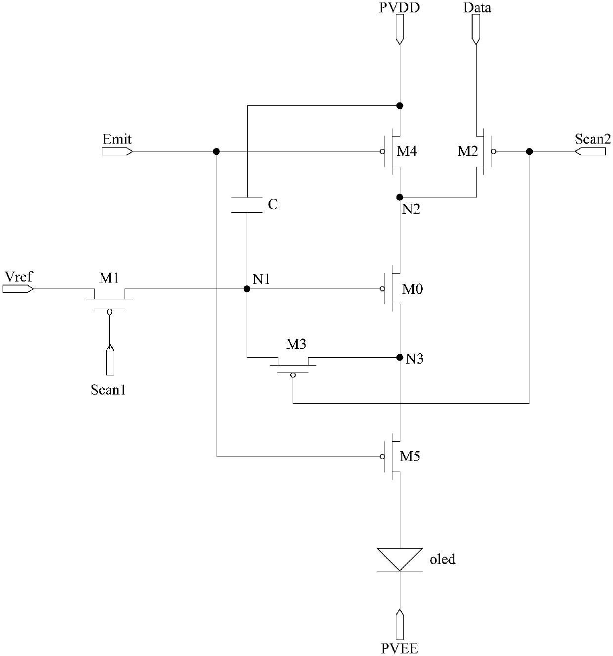
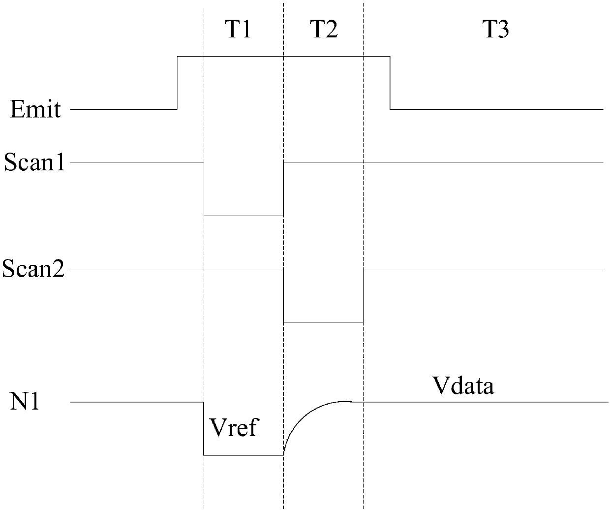
[0028] Organic light-emitting diodes (Organic light-emitting diodes, OLED) display panels have the advantages of low operating voltage, fast response speed, high luminous efficiency, wide viewing angle and wide operating temperature, which is conducive to thinning, low power consumption and curved surface design of display devices. . Moreover, in an OLED display panel, pixel circuits are usually used to drive the OLED to emit light. Pixel circuits usually reset the gate of the drive transistor before writing data to the OLED, e.g. figure 2 The pixel circuit shown, figure 2 A schematic circuit structure diagram of a pixel circuit provided by an embodiment of the present invention; it includes 5 switching transistors: M1-M5, 1 driving transistor M0 and 1 capacitor C. The corresponding input timing diagram is as follows figure 2 as shown, image 3 for figure 2 The corresponding input timing diagram for the pixel circuit shown. In the T1 phase, the first scan line Scan1 ...


PUM


Abstract

The invention discloses an OLED display panel and a display device. The OLED display panel comprises a display area, a middle area and a non-display area, wherein a second display area in the displayarea is divided into two display subareas by the middle area; and each first scanning line corresponding to pixels in the display subareas comprises a first subline extending along a row direction, asecond subline extending along the row direction and a third subline, wherein the first subline of the nth first scanning line is connected with the nth row of pixels, the second subline is connectedwith the (n+1)th row of pixels, and one end, close to the middle area, of the first subline is connected with the second subline through the third subline. That is to say, each first scanning line isformed by connecting the first subline, the second subline and the third subline in series, and each first scanning line is connected with two rows of pixels, so that pixel Loading on the scanning lines in each display subarea is close to that on the scanning lines in a first display area, and the problem of uneven display is solved.

Description

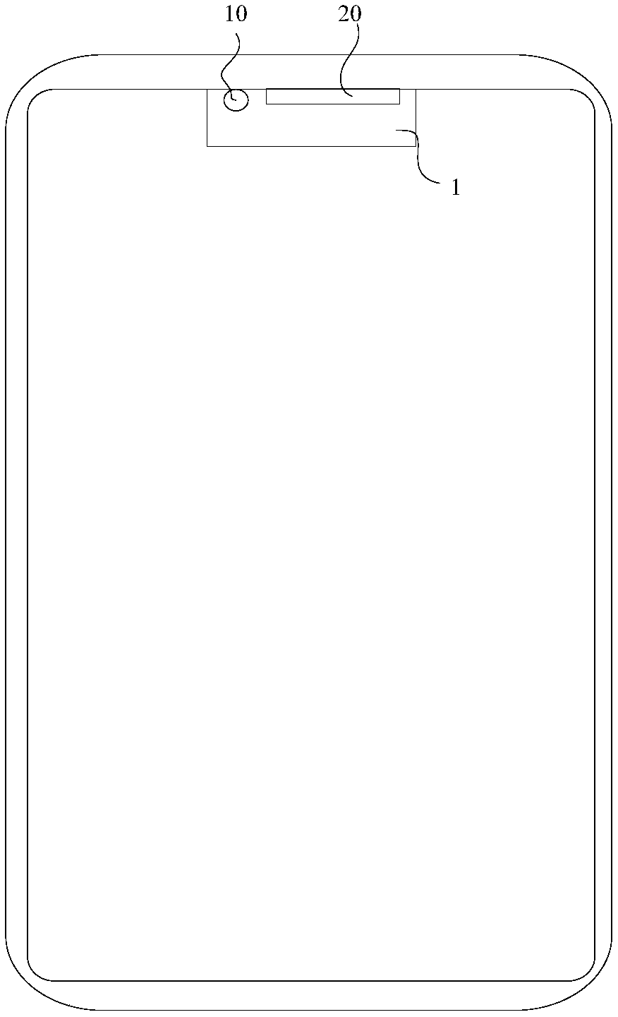
technical field [0001] The invention relates to the field of display technology, in particular to an OLED display panel and a display device. Background technique [0002] With the development of display technology, the full screen has a large screen-to-body ratio and an ultra-narrow bezel. Compared with ordinary display screens, it can greatly improve the visual effect of the viewer, and thus has received widespread attention. At present, in a display device with a full screen such as a mobile phone, in order to realize the functions of Selfie, video call and fingerprint recognition, a front camera, an earpiece, a fingerprint recognition area or physical buttons are usually arranged on the front of the display device. [0003] In order to achieve full-screen display, such as figure 1 In the schematic structural diagram of the display panel shown, a middle area 1 is set in the display area of ​​the display panel, and a front camera 10 , an earpiece 20 , etc. are set in the ...

Claims


Application Information

Patent Timeline
Patent Type & Authority Applications(China)
IPC IPC(8): H01L27/32
CPCH10K59/122H10K59/131
Inventor 杨轩
Owner WUHAN TIANMA MICRO ELECTRONICS CO LTD
Learn More